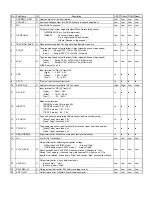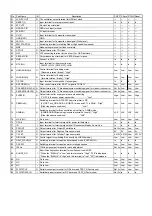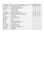
No.
Port Name
I/O
Description
P-OFF
P-Save
P-FAIL Reset
51
LC.OSC OUT
O The oscillation output terminal for OSD dot clock.
---
---
---
---
52
RESET(L)
I
Input terminal for microprocessor reset.
In
In
In
In
53
4FC.LPF
I
4fc clock input terminal
---
---
---
---
54
OSD.FSC IN
I
OSD clock input terminal
---
---
---
---
55
5V(OSD)
I
5V input terminal
---
---
---
---
56
CVIN
I
Input terminal for Composite video signal.
---
---
---
---
57
GND(OSD)
-- GND
---
---
---
---
58
LECHA
I
Input terminal for Composite video signal.(White level)
---
---
---
---
59
20M.START(H)
I
Switching terminal for stertting Mode.(High speed/Low speed)
---
---
---
---
60
MD0
I
Mode setting terminal for flash over-write.
---
---
---
---
61
CVOUT
O Output terminal for CG Video.
---
---
---
---
62
HLF
O LPF connecting terminal for the slicer. (For OSD dot clock.)
---
---
---
---
63
SECAM.V.IN
I
Chrominance input terminal for SECAM super impose.
---
---
---
---
64
GND
-- Connect to GND
In
In
In
In
65
S TAB(L)
I
Input terminal for the prevention tab.
[EXIST] :LOW [NO EXIST] :HIGH
In
In
In
In
66
UNLOADING(H)
O
Control terminal for loading motor.
[Reverse rotation / brake] : "High"
Low
Low
Low
Low
67
LOADING(H)
O
Control terminal for loading motor.
[forward rotation / brake] : "High"
Low
Low
Low
Low
68
C.SYNC
I
Input terminal for composite V-sync signal.
In
In
In
In
69
EX.FF/REW(L)
I
Filter control terminal for PB-CTL signal in FF/REW.
Low
Low
Low
Low
70
PAL-I/BG/DK(SYS4)
O Output terminal for TV broadcast system switching signal for video circuit control.
Not fix Low
Low
Low
71
SECAM/PAL(SYS2)
O Output terminal for TV broadcast system switching signal for video circuit control.
Not fix Low
Low
Low
72
SLEEP(L)
O
Output terminal for super power save mode setting.
P-OFF in the super power save mode……………… "Low".
High
Low
Low
High
73
PB60Hz(H)
O
Switching terminal for NTSC FM Audio trap filter in PB.
[VV (PB,Trick_PB/A-DUB, A-DUB-PS) mode and CTL is 60Hz] : "High"
[Other than above condition]
: "Low"
Low
Low
Low
Low
74
ADUB(H)
O
Switching terminal for Bias oscillation noise filter in A-DUB mode.
[ADUB/ADUB-PS(Including Assemble/syncro/AV-Insert)] : "High"
[Other than above condition]
: "Hi-Z"
Hi-Z
Hi-Z
Hi-Z
Hi-Z
75
N.C(VBI1)
-- Fix to Low.
Low
Low
Low
Low
76
P FAIL
I
Input terminal for Interrupt signal for power fail detection.
In
In
In
In
77
IR
I
Input terminal for Interrupt signal from IR sensor emitted by Remo-Con.
In
In
In
In
78
P50 OUT
O Output terminal for Project 50 serial data.
Not fix Low
Low
Low
79
CAP.ET
O Output terminal for Capstan Torque command.
0V
0V
Low
0V
80
CYL.ET
O Output terminal for Cylinder Torque command.
4.213V 4.213V Low
4.213V
81
DIGI.LINK
O Control signal for switching IR sensor.[only LOEWE model]
Low
Low
Low
Low
82
HALF_WAVE(H)
O Switching terminal for capstan driver speed mode.(FAST/SLOW)
In
In
In
In
83
CAP.R/F
O Switching terminal for capstan motor rotating direction.
Low
Low
Low
Low
84
125Hz
O 125Hz pulse output terminal for clock adjustment.
Not fix Low
Low
Low
85
SHORT_DN
I
Short Circuit detection terminal for oscillation circuit in REC.
*When the "BIAS(H)" is "Low" and this terminal is "High", "F08" is displayed.
*When the "BIAS(H)" is "High" and this terminal is "low", "F07" is displayed.
In
In
In
In
86
N.C
-- Fix to Low.
Low
Low
Low
Low
87
N.C
-- Fix to Low.
Low
Low
Low
Low
88
N.C
-- Fix to Low.
Low
Low
Low
Low
89
FLD/T2 CLK
O Serial clock output terminal for FIP driver and TEST_2(Factory use).
Not fix Low
Low
Low
90
FLD/T2 DATA IN
I
Serial data input terminal for FIP driver and TEST_2(Factory use).
Not fix In
In
In
Содержание NV-SJ220EG
Страница 18: ...http cxema ru 3 3 8 CIRCUIT BOARD LAYOUT ...
Страница 53: ...http cxema ru 10 2 CASING PARTS SECTION ...
Страница 54: ...http cxema ru 10 3 PACKING PARTS SECTION ...
Страница 55: ...http cxema ru 11 REPLACEMENT PARTS LIST 11 1 CHASSIS PARTS SECTION PARTS LIST ...
Страница 63: ...http cxema ru ...
Страница 65: ...http cxema ru ...
Страница 71: ...http cxema ru ...
Страница 73: ...http cxema ru ...
Страница 75: ...http cxema ru ...
Страница 77: ...http cxema ru ...


