background image

WPR1500-BUCK MP Receiver V2.1 Reference Design User’s Guide, Rev. 0, 09/2016

NXP Semiconductors

3


Hardware Description

5

Hardware Description

5.1

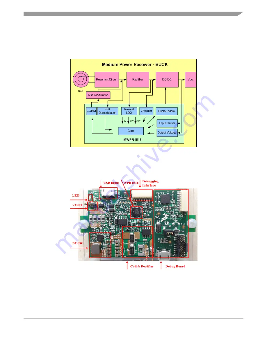
Reference board block diagram

Figure 3. WPR1500 receiver board block diagram – BUCK

5.2

Modules explanation

Figure 4. WPR1500-BUCK board modules overview

Содержание WPR1500-BUCK

Страница 1: ... has the capability to support future standards It is a low cost reference solution that can be easily customized using the FreeMASTER tool Figure 1 WPR1500 reference board BUCK Document Number WPR1500BUCKMPUG Rev 0 09 2016 Contents 1 Introduction 1 2 System Features 2 3 Package Checklist 2 4 System Block Diagram 2 5 Hardware Description 3 6 Getting Started 4 7 References 31 8 Revision History 31 ...

Страница 2: ...ction of rectifier voltage output voltage and output current Small PCB size 40 mm 40 mm FreeMASTER tool to enable customization and calibration 3 Package Checklist 4 System Block Diagram The WPR1500 medium power receiver wireless charging system is shown in Figure 2 Figure 2 Wireless charging system overview For the WPC Qi information visit www wirelesspowerconsortium com developers Table 1 Packag...

Страница 3: ...n User s Guide Rev 0 09 2016 NXP Semiconductors 3 Hardware Description 5 Hardware Description 5 1 Reference board block diagram Figure 3 WPR1500 receiver board block diagram BUCK 5 2 Modules explanation Figure 4 WPR1500 BUCK board modules overview ...

Страница 4: ...he following characteristics Input voltage 3 5 V 20 V AC peak Output voltage 3 5 V 20 V DC Communication The ASK differential bi phase signal is modulated by switching the modulation capacitor The FSK signal is demodulated by the CNC and FSKDT modules USB switch The CNC module automatically detects the input voltage from wired power plugs and switches on wired power when the input voltage is in th...

Страница 5: ...ng Started Figure 5 shows the connection diagram and Figure 6 shows a real setup Figure 5 Debug connections Figure 6 Development environment For details on the J Link debugger visit nxp com and search for J Link FreeMASTER J Link Debug board WPR1500 Receiver board 12 V 2 4 A DC adapter NXP MP Tx board ...

Страница 6: ... of the debug board and then connect the debug board to the receiver board using a 10 pin cable NOTE The micro interface on the debug board must be connected to the USB to receive power Ensure that the jumper J110 is connected before the download The J Link connection is shown in Figure 7 Figure 7 J Link connection When the J Link is plugged into the PC it can be found in Windows Device Manager as...

Страница 7: ...WPR1500 BUCK MP Receiver V2 1 Reference Design User s Guide Rev 0 09 2016 NXP Semiconductors 7 Getting Started Figure 8 J Link debugger plugged in Figure 9 P E Multilink debugger plugged in ...

Страница 8: ...f the wireless charger application project you can open the application project and build the applications directly whenever the wpr_lib a is ready The configurations in MWPR1516_config h are set for the BUCK board by default To build this project for the LDO board change the macro definition BOARD_OUT_TYPE from define BOARD_OUT_TYPE OUT_TYPE_BUCK to define BOARD_OUT_TYPE OUT_TYPE_LDO Then rebuild...

Страница 9: ...hen the build is complete the IAR displays this information in the build window Figure 11 Successfull build of a project 3 Ensure that the debugger is configured properly in the project options Select the flash loader to support downloading of the binary to the internal flash Figure 12 Flash loader configuration ...

Страница 10: ...09 2016 10 NXP Semiconductors Getting Started When using J Link as a debugger select J link J Trace Figure 13 J Link debugger configuration for driver When using P E Multilink as a debugger select the PE micro Figure 14 P E Multilink debugger configuration for driver ...

Страница 11: ... micro settings as shown in Figure 15 Figure 15 Debugger configuration for PE micro 4 Download the project After the application is built successfully click the Download and Debug button to download the application to the target device Figure 16 Download and Debug button The programming of a project is shown in Figure 17 Figure 17 Programming a project ...

Страница 12: ... driver library is already included in the library folder and platform folder of the wireless charger application project you can open the application project and build the applications directly whenever the wpr_lib lib is ready The configurations in MWPR1516_config h are set for the BUCK board by default To build this project for the LDO board change the macro definition BOARD_OUT_TYPE from defin...

Страница 13: ...ence Design User s Guide Rev 0 09 2016 NXP Semiconductors 13 Getting Started Figure 19 Building a project When the build is complete KEIL displays this information in the build window as follows Figure 20 Building a project successfully ...

Страница 14: ...miconductors Getting Started 3 Ensure that the debugger configuration is correct in the project options The flash loader must be selected to support downloading the binary to the internal Flash Figure 21 Flash loader configurations If using the J Link as debugger choose J link J Trace ...

Страница 15: ... BUCK MP Receiver V2 1 Reference Design User s Guide Rev 0 09 2016 NXP Semiconductors 15 Getting Started Figure 22 Debugger configurations for J Link If using P E Multilink as the debugger choose the PE micro ...

Страница 16: ...16 16 NXP Semiconductors Getting Started Figure 23 Debugger configurations for PE micro 4 Download the project After the application is built successfully click the Download button to download the application to the target device Figure 24 Download button Program a project ...

Страница 17: ...ide Rev 0 09 2016 NXP Semiconductors 17 Getting Started Figure 25 Programming a project 5 After the application is downloaded to the target device click Start Stop Debug Session to debug the code The debugger stops executing at the start of the main function ...

Страница 18: ...al components Because the receiver driver library is already included in the lib folder and platform folder of the wireless charger application project you can open the application project and build the applications directly whenever the libwpr_lib a is ready The configurations in MWPR1516_config h are set for the BUCK board by default To build this project for the LDO board change the macro defin...

Страница 19: ...ceiver V2 1 Reference Design User s Guide Rev 0 09 2016 NXP Semiconductors 19 Getting Started Figure 27 Build the project When the build is complete CodeWarrior displays this information in the Console window as follows ...

Страница 20: ...wo supported debugger settings are already configured in the project Figure 29 Flash loader configurations When using the J Link as the debugger select WPR1500_REF_FLASH_Segger Jlink_Trace When using the P E Multilink as the debugger select WPR1500_REF_FLASH_PnE U MultiLink If you want to change some parameters click the Edit button in the Target setting subpage The configuration interface is show...

Страница 21: ...1 Getting Started Figure 30 Debug configurations 4 Download and debug the project After the application is built successfully click the Debug button in the above mentioned configuration dialog Then the project code is downloading and the debugger stops executing at the start of the main function ...

Страница 22: ...ng Started Figure 31 Stop at main when running debugging 6 3 Debugging the WPR1500 receiver using FreeMASTER 6 3 1 Connecting the debug cable The FreeMASTER debug connection is shown in Figure 32 Ensure that the jumper J110 is removed before debugging and then put the receiver on the transmitter panel ...

Страница 23: ...iconductors 23 Getting Started Figure 32 FreeMASTER debug connection 6 3 2 Setting FreeMASTER project options 1 Set the symbol file for your project Select a symbol file from FreeMASTER Project Options MAP Files as shown in the following figure The IAR project is used as an example ...

Страница 24: ...16 24 NXP Semiconductors Getting Started Figure 33 Selecting a symbol file 2 Select a communication interface for FreeMASTER Select Plug in Module in FreeMASTER Project Options Comm as shown in the following figure Then select FreeMASTER Segger Jlink Communication Plug in ...

Страница 25: ...rovides the FreeMASTER GUI tool to monitor the system working status Open WPR1500_REF pmp with this tool start up the RX board and click the red Start Stop button For the FreeMASTER tool visit nxp com Freemaster The FreeMASTER GUI can be used to monitor the system state and change some parameters manually if necessary The user can get the system error code through the oscilloscope in the GUI ...

Страница 26: ...k the Store to flash button to save these parameters in flash These parameters are used to calibrate the output current every time when the RX board is started The internal PGA calibration function is disabled by default because of the flash limitation When this function is enabled the calibration result can also be saved in flash by default The FOD Calibration function can work offline The user n...

Страница 27: ...he system manually when RX works properly It can set the expected Vrec voltage enable or disable output set the control error packet value and so on This function is useful to debug the system in details Figure 36 Control page of the FreeMASTER GUI 6 4 Testing 6 4 1 Signals on the board The main signals on the WPR1500 reference board are shown in Figure 37 ...

Страница 28: ... as follows TP6 USB input voltage TP9 VREC TP7 TP8 GND TP12 DC DC output enable The following examples show how to measure and debug the board follow 1 Figure 38 shows the input voltage and communication signal from ping phase to power transfer setup Channel 1 rectifier DC output voltage VREC Channel 2 coil AC input voltage V_Coil Channel 3 communication signal CTX Channel 4 coil AC input current ...

Страница 29: ...nce Design User s Guide Rev 0 09 2016 NXP Semiconductors 29 Getting Started Figure 38 Ping process of the wireless power receiver 2 System response measurement for a 3 A load is shown in Figure 39 Figure 39 System response for a 3 A load ...

Страница 30: ...tarted 3 System response measurement for adding the load gradually from 0 A is shown in Figure 40 Figure 40 System response for adding loading gradually 4 System response measurement for reducing the load from 3 A to 0 A is shown in Figure 41 Figure 41 System response for reducing the load from 3 A to 0 A ...

Страница 31: ...erences NXP wireless charging solution page nxp com wirelesscharging NXP FreeMASTER tool page nxp com Freemaster WPC page www wirelesspowerconsortium com 8 Revision History This table summarizes revisions to this document Table 2 Revision history Revision number Date Substantive changes 0 09 2016 Initial release ...

Страница 32: ... incidental damages Typical parameters that may be provided in Freescale data sheets and or specifications can and do vary in different applications and actual performance may vary over time All operating parameters including typicals must be validated for each customer application by customer s technical experts Freescale does not convey any license under its patent rights nor the rights of other...

Страница 33: ...Mouser Electronics Authorized Distributor Click to View Pricing Inventory Delivery Lifecycle Information NXP WPR1500 HV ...

Отзывы: