


NXP Semiconductors
UM11623
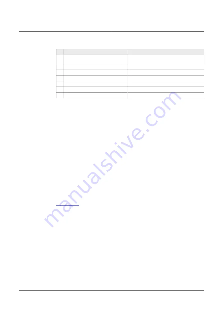
PCA9959HN-ARD evaluation board
J46 Fuji output connector (top)
J47 Fuji input connector (top)
6
SDO (U2) distribution to next board SDI
(U2)
6
SDO (U2) from previous board
7
OE distribution
7
OE distribution
8
SDO (U2) from last board to SPI-MISO
8
SDO (U2) from next board (SDO bridge)
9
SPI – CS distribution
9
SPI – CS distribution
10 SPI – CLOCK distribution
10 SPI – CLOCK distribution
11 GND
11 GND
12 GND
12 GND
Table 3. Pin chart of Fuji connectors and their functions
...continued
5.6 SPI bus
The SPI bus has a daisy chain architecture. When a single daughter board (inserted
in the Arduino port) is used, the MOSI line (J36, pin 4) goes from Arduino port to the
DUT SDI input (U2, pin 6). The signal is turned back from SDO (U2, pin 4) through
the switch U5 (closed), to the MISO input of the Arduino port (J36, pin 5). U5 is closed
because the control input is pulled up (high state) through R89. When a secondary board
is inserted into the Fuji output connector, the U5 control input located on the first board
is pulled down to ground through pin 3 of J46 and J47 of the next board. The switch U5
(first board) is open, the signal path of the SPI is: MOSI (Arduino port) – SDI input (U2,
first board) – SDO output (U2, first board) – pin 6 (J46 first board) – pin 6 (J47 second
board) – SDI (U2, second board) – SDO (U2, second board) – U5 (second board which is
closed) – pin 8 (J47, second board) – pin 8 (J46, first board) – MISO (Arduino port). The
daisy chain loop is then closed through both DUTs on the two interconnected daughter
boards. The SPI clock and chip select lines are sent directly to the DUT (U2) on the first
card, and through the Fuji connectors to the secondary card.
For SPI characteristics and data format, see the PCA9959 data sheet Table 1 and Table
2, which details the pin map of the Arduino port and the Fuji connectors.
Note:
For IMXRT1050 EVK, the SPI lines on the EVK board are not linked to the
Arduino connector. Before using the EVK, the user must populate the DNP 0 Ω resistors
R278 to R281 (see the EVK schematic diagram file SPF-30168_A1.pdf, available at
.
UM11623
All information provided in this document is subject to legal disclaimers.
© NXP B.V. 2021. All rights reserved.
User manual
Rev. 1 — 21 May 2021
9 / 32