NXP Semiconductors PCA9665 Скачать руководство пользователя страница 77

PCA9665_2

© NXP B.V. 2006. All rights reserved.

Product data sheet

Rev. 02 — 7 December 2006

77 of 91

NXP Semiconductors

PCA9665

Fm+ parallel bus to I

2

C-bus controller

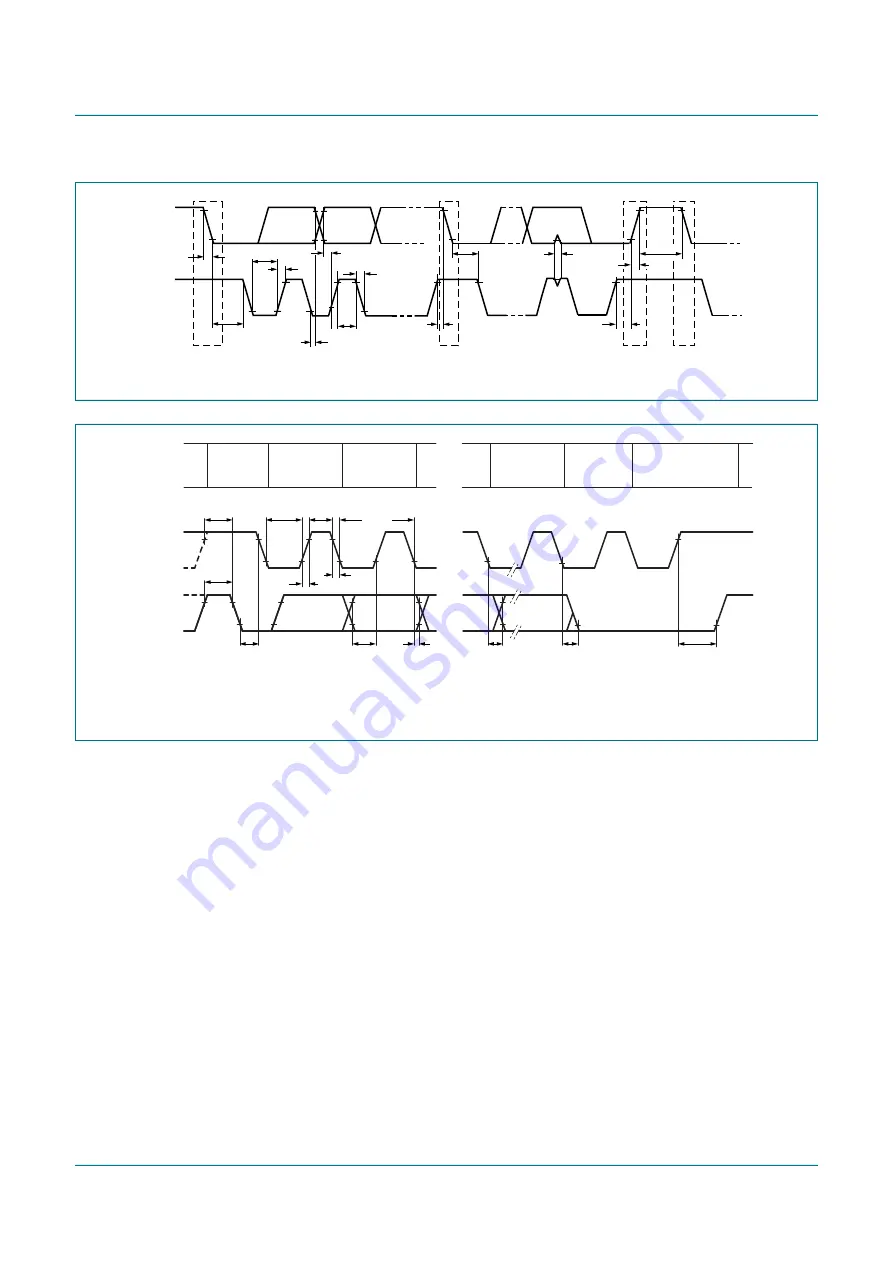
Fig 41. Definition of timing on the I

2

C-bus

SDA

SCL

002aab271

t

f

S

Sr

P

S

t

HD;STA

t

LOW

t

r

t

SU;DAT

t

f

t

HD;DAT

t

HIGH

t

SU;STA

t

HD;STA

t

SP

t

SU;STO

t

r

t

BUF

Rise and fall times refer to V

IL

 and V

IH

.

Fig 42. I

2

C-bus timing diagram

SCL

SDA

t

HD;STA

t

SU;DAT

t

HD;DAT

t

f

t

BUF

t

SU;STA

t

LOW

t

HIGH

t

VD;ACK

002aac696

protocol

START

condition

(S)

bit 7

MSB

bit 6

bit n

bit 0

acknowledge

(A)

1

/f

SCL

t

r

t

VD;DAT

t

SU;STO

STOP

condition

(P)

Содержание PCA9665

Страница 1: ...CL SDA 68 byte buffer I2C bus General Call Software reset on the parallel bus 2 Features n Parallel bus to I2C bus protocol converter and interface n Both master and slave functions n Multi master cap...

Страница 2: ...ing to run a large number of traces across the entire printed circuit board 4 Ordering information Table 1 Ordering information Tamb 40 C to 85 C Type number Topside mark Package Name Description Vers...

Страница 3: ...TROL BLOCK CE WR RD INT RESET A1 A0 VDD A1 A0 0 1 0 0 0 0 1 1 INTERRUPT CONTROL POWER ON RESET D7 D6 D5 D4 D3 D2 D1 D0 data FILTER control signals 002aab023 BIT7 BIT6 BIT5 BIT4 BIT3 BIT2 BIT1 BIT0 IND...

Страница 4: ...D5 D6 D7 i c 1 2 3 4 5 6 7 8 9 10 12 11 14 13 16 15 18 17 20 19 VDD SDA SCL RESET INT A1 A0 CE RD WR PCA9665PW D0 002aab021 1 2 3 4 5 6 7 8 9 10 12 11 14 13 16 15 18 17 20 19 VSS D1 D2 D3 D4 D5 D6 D7...

Страница 5: ...Supply ground WR 11 8 I Write strobe When LOW and CE is also LOW the content of the data bus is loaded into the addressed register Data are latched on the rising edge of either WR or CE RD 12 9 I Read...

Страница 6: ...are selected by setting pins A0 and A1 to the appropriate logic levels before a read or write operation is executed on the parallel bus The seven indirect registers require that the INDPTR indirect r...

Страница 7: ...W 86h I2CTO time out 04h R W FFh I2CPRESET parallel software reset 05h W 00h I2CMODE I2C bus mode 06h R W 00h Fig 6 Register mapping flowchart 002aab459 I2CSTA REGISTER A1 A0 00 read yes no INDPTR RE...

Страница 8: ...in Table 4 7 3 1 3 The I2C bus Data register I2CDAT A1 0 A0 1 I2CDAT is an 8 bit read write register It contains a byte of serial data to be transmitted or a byte which has just been received In maste...

Страница 9: ...ster Two bits are affected by the bus controller hardware the SI bit is set when a serial interrupt is requested and the STO bit is cleared when a STOP condition is present on the I2C bus A Write to t...

Страница 10: ...665 enters the not addressed Slave Receiver mode and the SDA line remains at a HIGH level In state C8h the AA flag can be set again for future address recognition When the PCA9665 is in the not addres...

Страница 11: ...o START condition or repeated START condition will be generated 4 STO The STOP flag STO 1 When the STO bit is set while the bus controller is in a master mode a STOP condition is transmitted on the I2...

Страница 12: ...ifferent from the General Call address 000 0000 for proper device operation Table 13 I2CCOUNT Byte Count register indirect address 00h bit allocation 7 6 5 4 3 2 1 0 LB BC6 BC5 BC4 BC3 BC2 BC1 BC0 Tab...

Страница 13: ...period 35 ns 5 ns Remark The I2CMODE register needs to be programmed before programming the I2CSCLL and I2CSCLH registers in order to know which I2C bus mode is selected See Section 7 3 2 6 The I2C b...

Страница 14: ...every time the SCL goes LOW If SCL stays LOW for a time period equal to or greater than the time out value the bus controller concludes there is a bus error and behaves in the manner described above...

Страница 15: ...e minimum values that can be used for the corresponding I2C bus mode Use of lower values will cause the minimum values to be loaded 2 Using the formula Table 23 I2CMODE I2C bus Mode register indirect...

Страница 16: ...mission and lets the PCA9665 perform it without having to access the Status Register and the Control Register each time a single command is performed The microcontroller can then perform other tasks w...

Страница 17: ...Byte mode can be entered I2CCON must be initialized as shown in Table 26 ENSIO must be set to logic 1 to enable the PCA9665 If the AA bit is reset the PCA9665 will not acknowledge its own slave addres...

Страница 18: ...d with AA 1 D8h if the PCA9665 lost the arbitration and is addressed as a slave receiver during a General Call sequence slave mode enabled with AA 1 and General Call address enabled with GC 1 in I2CAD...

Страница 19: ...A P 30h F8h A P 20h F8h 002aab024 A or A 38h other MST continues A or A 38h other MST continues A B0h other MST continues 68h to corresponding states in Slave Transmitter mode to corresponding states...

Страница 20: ...0 0 X 0 Repeated START will be transmitted no I2CDAT action or 0 1 0 X 0 STOP condition will be transmitted STO flag will be reset no I2CDAT action 1 1 0 X 0 STOP condition followed by a START condit...

Страница 21: ...l be reset no I2CDAT action 1 1 0 X 0 STOP condition followed by a START condition will be transmitted STO flag will be reset 38h Arbitration lost in SLA W or Data bytes No I2CDAT action or 0 0 0 0 0...

Страница 22: ...When the slave address and the data direction bit have been transmitted the serial interrupt flag SI is set again the Interrupt line INT goes LOW again and I2CSTA is loaded with the following possible...

Страница 23: ...r Transmitter mode entry MT 4 A P 48h F8h 002aab025 A 38h other MST continues A or A 38h other MST continues A other MST continues successful reception from a Slave Transmitter next transfer started w...

Страница 24: ...n the bus becomes free 40h SLA R has been transmitted ACK has been received No I2CDAT action or 0 0 0 0 0 Data byte will be received NACK bit will be returned no I2CDAT action 0 0 0 1 0 Data byte will...

Страница 25: ...followed by the data direction bit which must be 0 W to operate in the Slave Receiver mode After its own slave address and the W bit have been received the Serial Interrupt flag SI is set the Interru...

Страница 26: ...more data bytes all are Acknowledged last data byte received is Not Acknowledged arbitration lost as MST and addressed as slave DATA A 80h P or S F8h A 88h on STOP P or S F8h on STOP GENERAL CALL 00h...

Страница 27: ...rbitration lost in SLA R W as master General Call address has been received ACK bit has been returned No I2CDAT action or X X 0 0 0 Data byte will be received and NACK will be returned no I2CDAT actio...

Страница 28: ...0 0 1 0 Switched to not addressed slave mode own slave address will be recognized General Call address will be recognized if GC 1 A START condition will be transmitted when the bus becomes free A0h A...

Страница 29: ...byte of the transfer and enter state C8h The PCA9665 is switched to the not addressed slave mode and will ignore the master receiver if it continues the transfer Thus the master receiver receives all...

Страница 30: ...0 X 0 0 0 Switched to not addressed slave mode no recognition of own slave address General Call address recognized if GC 1 no I2CDAT action or 0 X 0 1 0 Switched to slave mode Own slave address will...

Страница 31: ...ber of data bytes to be sent The byte count register I2CCOUNT has been previously programmed with the number of bytes that need to be sent in a single sequence BC 6 0 as shown in Table 34 LB bit is on...

Страница 32: ...itration and is addressed as a slave transmitter slave mode enabled with AA 1 68h if the PCA9665 lost the arbitration and is addressed as a slave receiver slave mode enabled with AA 1 D8h if the PCA96...

Страница 33: ...tates in the Master Transmitter Buffered mode MODE 1 08h S SLA W A DATA A P 28h F8h MT 10h S SLA W R to MST REC mode entry MR 5 A P 30h F8h A P 20h F8h 002aab659 A or A 38h other MST continues A or A...

Страница 34: ...a bytes X X 0 X 1 SLA W will be transmitted If ACK bit received data bytes will be transmitted until all of them have been sent and an ACK has been received for each of them or until a NACK bit is rec...

Страница 35: ...OP condition followed by a START condition will be transmitted STO flag will be reset 30h Up to BC 6 0 bytes in I2CDAT have been transmitted NACK has been received for the last byte Load the data byte...

Страница 36: ...rite to I2CCON resets the SI bit clears the Interrupt INT goes HIGH and allows the serial transfer to continue When the slave address and the data direction bit have been transmitted and all the data...

Страница 37: ...A P 50h F8h MR 10h S SLA R W to Master Transmitter mode entry MT 5 A P 48h F8h 002aab660 A 38h other MST continues A or A 38h other MST continues A other MST continues successful reception from a Sla...

Страница 38: ...es will be received ACK bit will be returned for all of them except for the last one where NACK bit will be returned 10h A repeated START condition has been transmitted Load SLA R or 0 Total number of...

Страница 39: ...will be received ACK bit will be returned for all of them Read data bytes or 1 Total number of bytes to be received 0 0 0 X 1 BC 6 0 data bytes will be received ACK bit will be returned for all of th...

Страница 40: ...its own slave address followed by the data direction bit which must be 0 W to operate in the Slave Receiver mode After its own slave address and the W bit have been received the Serial Interrupt flag...

Страница 41: ...bytes received is equal to the value in I2CCOUNT register and LB 0 3 Defined state when the number of bytes received is equal to the value in I2CCOUNT register and LB 1 4 Number of bytes received is l...

Страница 42: ...master Own SLA W has been received ACK has been returned No I2CDAT action or 0 Total number of bytes to be received X X 0 X 1 Up to BC 6 0 data bytes will be received ACK bit will be returned for all...

Страница 43: ...es or X X 0 X 0 0 1 Switched to not addressed slave mode No recognition of own slave address General Call address will be recognized if GC 1 Read data bytes or X X 0 X 0 1 1 Switched to not addressed...

Страница 44: ...zed if GC 1 A START condition will be transmitted when the bus becomes free Read data bytes X X 1 X 0 1 1 Switched to not addressed slave mode Own slave address will be recognized General Call address...

Страница 45: ...PCA9665 will transmit all the bytes of the transfer values defined by BC 6 0 and enter state C8h The PCA9665 is switched to the not addressed slave mode and will ignore the master receiver if it cont...

Страница 46: ...ata bytes or X Total number of data bytes to be transmitted X X 0 0 1 Up to BC 6 0 bytes will be transmitted PCA9665 switches to the not addressed mode after BC 6 0 bytes have been transmitted Load da...

Страница 47: ...ssed slave mode No recognition of own slave address General Call address recognized if GC 1 No I2CDAT action or X X 0 X 0 1 1 Switched to slave mode Own slave address will be recognized General Call a...

Страница 48: ...register is performed 4 After reading the I2CSTA status register the I2CCON is programmed with STA 0 That clears the previous Interrupt If a START command has been previously sent the first byte load...

Страница 49: ...ot been sent To be able to end the reception the last buffered sequence must be performed with LB 1 Master Receiver Buffered mode ends when the I2CCOUNT register is programmed with STO 1 8 5 3 Buffere...

Страница 50: ...the I2C bus master MODE bit must be set to 1 each time a write to the I2CCON register is performed 4 When the sequence has been executed BC 6 0 bytes have been received or the master sent a STOP or Re...

Страница 51: ...5 10 Program I2CCOUNT C0h 64 bytes and Last byte is not acknowledged 11 Program I2CCON with STA STO SI 0 MODE 1 12 The PCA9665 reads 64 bytes and does not acknowledge the last byte the PCA9665 sends a...

Страница 52: ...th byte n if there was no interrupt after slave address was sent n 1 if there was an interrupt after slave address was sent Master Receiver Buffered mode After START condition don t care After Slave A...

Страница 53: ...Table 43 Own slave address General Call address and Data acknowledge management AA GC LB MODE Address Data received 1 Master mode the PCA9665 generates a START command and controls the I2C bus 0 X X...

Страница 54: ...itter mode NACK returned after own slave address received switch to not addressed slave mode any time during an I2C bus sequence Slave Receiver mode NACK returned after own slave address received NACK...

Страница 55: ...o non addressed mode after the last byte of a buffered sequence is transmitted after bytes sent BC 6 0 value Slave Receiver mode NACK returned after own slave address received in addressed mode data a...

Страница 56: ...ave Transmitter mode ACK returned after own slave address received in addressed mode data are transmitted on a multiple byte basis BC 6 0 value always addressed during a buffered sequence Slave Receiv...

Страница 57: ...ntroller must send an external hardware or software reset signal to reset the PCA9665 8 8 3 I2CSTA 70h This status code indicates that the SDA line is stuck LOW when the PCA9665 in master mode is tryi...

Страница 58: ...he following states in I2CSTA 38h 68h and B0h see Figure 7 Figure 11 Figure 8 and Figure 12 Remark In order to exit state 38h a Time out Reset or external STOP are required If the STA flag in I2CCON i...

Страница 59: ...L line see Figure 17 The PCA9665 sends out nine clock pulses followed by the STOP condition If the SDA line is released by the slave pulling it LOW a normal START condition is transmitted by the PCA96...

Страница 60: ...ower is applied to VDD an internal Power On Reset holds the PCA9665 in a reset condition until VDD has reached VPOR At this point the reset condition is released and the PCA9665 goes to the power up i...

Страница 61: ...in master slave functions Fig 18 Parallel Software Reset sequence 002aab966 A 1 0 00 10 access to INDPTR Indirect Register pointer access to the INDIRECT Indirect Data field D 7 0 05h I2CPRESET regist...

Страница 62: ...master receiver reads data from PCA9665 1 As defined in I2CADR register Fig 21 Bus timing diagram Unbuffered Slave Transmitter mode n byte ACK SCL SDA INT START condition 7 bit address 1 R W 1 interru...

Страница 63: ...and number of bytes sent value programmed in I2CCOUNT register BC 6 0 68 Fig 23 Bus timing diagram Buffered Master Transmitter mode n byte 1 ACK SCL SDA INT START condition 7 bit address 1 R W 0 from...

Страница 64: ...TOP condition 002aab269 from master receiver interrupt interrupt Slave PCA9665 is written to by external master transmitter 1 As defined in I2CADR register 2 Number of bytes received value programmed...

Страница 65: ...d of the clock pulse as changes in the data line at this time will be interpreted as control signals see Figure 28 9 1 1 START and STOP conditions Both data and clock lines remain HIGH when the bus is...

Страница 66: ...ve transmitter The device that acknowledges has to pull down the SDA line during the acknowledge clock pulse so that the SDA line is stable LOW during the HIGH period of the acknowledge related clock...

Страница 67: ...CA9665 can also be used to add more I2C bus ports to smart devices provide a higher frequency lower voltage migration path for the PCF8584 and convert 8 bits of parallel data to a serial bus to avoid...

Страница 68: ...ferent buses so that each bus can operate at its maximum potential 10 4 Convert 8 bits of parallel data into I2C bus serial data stream Functioning as a slave transmitter the PCA9665 can convert 8 bit...

Страница 69: ...ate voltage tolerance on inputs and outputs when no supply voltage is present Table 47 Limiting values In accordance with the Absolute Maximum Rating System IEC 60134 Symbol Parameter Conditions Min M...

Страница 70: ...RESET VIL LOW level input voltage 0 0 8 V VIH HIGH level input voltage 1 2 0 5 5 V IL leakage current input VI 0 V or 5 5 V 1 1 A Ci input capacitance VI VSS or VDD 2 0 3 pF Inputs outputs D0 to D7 VI...

Страница 71: ...DA and SCL bus Table 49 Dynamic characteristics 3 3 volt 1 2 3 VCC 3 3 V 0 3 V Tamb 40 C to 85 C unless otherwise specified See Table 50 on page 72 for 2 5 V Symbol Parameter Conditions Min Typ Max Un...

Страница 72: ...Table 50 Dynamic characteristics 2 5 volt 1 2 3 VCC 2 5 V 0 2 V Tamb 40 C to 85 C unless otherwise specified See Table 49 on page 71 for 3 3 V Symbol Parameter Conditions Min Typ Max Unit Initializat...

Страница 73: ...XP Semiconductors PCA9665 Fm parallel bus to I2C bus controller Fig 36 Reset timing SDA SCL 002aab272 trst 50 30 50 50 30 trec rst tw rst RESET Dn Dn off START trst ACK or read cycle 30 Dn on 30 Fig 3...

Страница 74: ...parallel bus to I2C bus controller Fig 38 Bus timing read cycle Fig 39 Parallel bus timing write cycle A0 to A1 CE RD D0 to D7 read 002aac693 tsu A th A tsu CE_N th CE_N tw RDL tw RDH float float not...

Страница 75: ...roller VM 1 5 V VX VOL 0 3 V VY VOH 0 3 V VOL and VOH are typical output voltage drops that occur with the output load Fig 40 Data timing 002aab274 td QLZ td QHZ outputs floating outputs enabled outpu...

Страница 76: ...filters on the SDA and SCL inputs suppress noise spikes less than 50 ns Table 51 I2C bus frequency and timing specifications All the timing limits are valid within the operating supply voltage and amb...

Страница 77: ...ng on the I2C bus SDA SCL 002aab271 tf S Sr P S tHD STA tLOW tr tSU DAT tf tHD DAT tHIGH tSU STA tHD STA tSP tSU STO tr tBUF Rise and fall times refer to VIL and VIH Fig 42 I2C bus timing diagram SCL...

Страница 78: ...ta Test Load S1 CL RL td DV 50 pF 500 VDD 2 td QZ 50 pF 500 open Test data are given in Table 53 RL load resistance RL for SDA and SCL 1 k 3 mA or less current CL load capacitance includes jig and pro...

Страница 79: ...e original mm dimensions SOT146 1 99 12 27 03 02 13 A min A max b Z max w ME e1 1 73 1 30 0 53 0 38 0 36 0 23 26 92 26 54 6 40 6 22 3 60 3 05 0 254 2 54 7 62 8 25 7 80 10 0 8 3 2 4 2 0 51 3 2 0 068 0...

Страница 80: ...27 10 65 10 00 1 1 1 0 0 9 0 4 8 0 o o 0 25 0 1 DIMENSIONS inch dimensions are derived from the original mm dimensions Note 1 Plastic or metal protrusions of 0 15 mm 0 006 inch maximum per side are n...

Страница 81: ...5 0 80 0 30 0 19 0 2 0 1 6 6 6 4 4 5 4 3 0 65 6 6 6 2 0 4 0 3 0 5 0 2 8 0 o o 0 13 0 1 0 2 1 DIMENSIONS mm are the original dimensions Notes 1 Plastic or metal protrusions of 0 15 mm maximum per side...

Страница 82: ...1 5 1 4 9 3 25 2 95 e1 2 6 e2 2 6 0 38 0 23 0 05 0 00 0 05 0 1 DIMENSIONS mm are the original dimensions SOT662 1 MO 220 0 75 0 50 L 0 1 v 0 05 w 0 2 5 5 mm scale SOT662 1 HVQFN20 plastic thermal enha...

Страница 83: ...torage temperature Tstg max If the printed circuit board has been pre heated forced cooling may be necessary immediately after soldering to keep the temperature within the permissible limit 17 2 2 Man...

Страница 84: ...ering see Figure 49 For further information on temperature profiles refer to Application Note AN10365 Surface mount reflow soldering description Table 54 SnPb eutectic process from J STD 020C Package...

Страница 85: ...at a 45 angle to the transport direction of the printed circuit board The footprint must incorporate solder thieves downstream and at the side corners During placement and before soldering the package...

Страница 86: ...board and the heatsink On versions with the heatsink on the top side the solder might be deposited on the heatsink surface 7 If wave soldering is considered then the package must be placed at a 45 ang...

Страница 87: ...ntroller Table 12 I2CCON Control register A1 1 A0 1 bit description description of bit 6 4th paragraph changed it takes 550 s for the internal oscillator to start up to it takes 550 s enable time for...

Страница 88: ...to 13 ns changed Min value for tw RDL from 9 ns to 20 ns changed Min value for tw WRL from 9 ns to 20 ns changed Min value for tsu Q from 8 ns to 12 ns changed Min value for tw RDH from 12 ns to 18 n...

Страница 89: ...ns where failure or malfunction of a NXP Semiconductors product can reasonably be expected to result in personal injury death or severe property or environmental damage NXP Semiconductors accepts no l...

Страница 90: ...eceiver Byte mode 25 8 3 4 Slave Transmitter Byte mode 29 8 4 Buffered mode 31 8 4 1 Master Transmitter Buffered mode 31 8 4 2 Master Receiver Buffered mode 36 8 4 3 Slave Receiver Buffered mode 40 8...

Страница 91: ...n 12 Static characteristics 70 13 Dynamic characteristics 71 14 Test information 78 15 Package outline 79 16 Handling information 83 17 Soldering 83 17 1 Introduction 83 17 2 Through hole mount packag...

Отзывы: