


NXP Semiconductors
UM11762
NTS0304EUK-ARD evaluation board
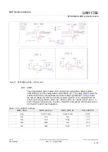
Figure 3. NTS0304EUK-ARD – Arduino connectors
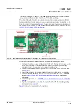
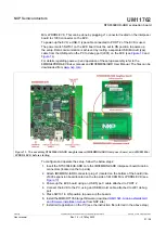
4.6 Level translator
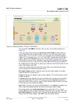
From the Arduino interface, the SPI and I
2
C-bus are connected to PORT B of the 4-bit
level translator U7. The are six total bus lines, therefore the SDA / SCL lines of the I
2
C-
bus are multiplexed with MOSI / SCLK of SPI bus. The signal switch is realized with
74HCT4053D (U5). PORT B of U7 is set to 3.3 V, the logic level of the Arduino interface.
From PORT A of U7, the signals go to PORT A of U6 (the DUT) through the jumper
header J8. PORT A of both level translators U6 and U7 are supplied from programmable
power supply “LDO1”. The output enable input of U6 is set with the jumper header J7.
The OE input of U7 is set HIGH (OE active).
After the level shift, the signal lines go from PORT B of the DUT to PORT A of the level
translators U8 and U10, through the jumper header J9. The jumper headers J8 and J9
isolate the pins of U6 from the circuit and can be used for direct access from external
to the IO lines of the DUT. PORT B of U6 along with the PORT A of U8 and U10 are
supplied from “LDO2”.
PORT B of level translators U8 and U10 is connected to digital potentiometer U11.
The lines also return to the Arduino interface (the IO lines D6 to D9), in a loopback
configuration. This allows the ability to test the bidirectional capability of the DUT.
depicts the entire path for signal lines.
UM11762
All information provided in this document is subject to legal disclaimers.
© NXP B.V. 2022. All rights reserved.
User manual
Rev. 1.0 — 27 May 2022
9 / 29