


UM10800
All information provided in this document is subject to legal disclaimers.
© NXP Semiconductors N.V. 2016. All rights reserved.
User manual
Rev. 1.2 — 5 October 2016
326 of 487
NXP Semiconductors
UM10800
Chapter 21: 12-bit Analog-to-Digital Converter (ADC)
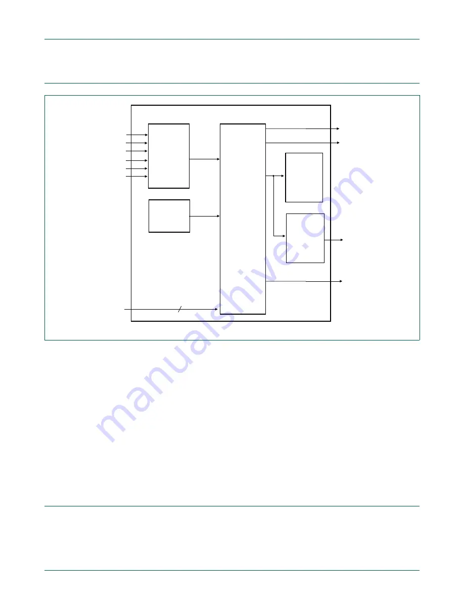
21.5 General description
The ADC controller provides great flexibility in launching and controlling sequences of A/D
conversions using the associated 12-bit, successive approximation A/D converter. A/D
conversion sequences can be initiated under software control or in response to a selected
hardware trigger. The ADC supports eight hardware triggers.
Once the triggers are set up (software and hardware triggers can be mixed), the ADC runs
through the pre-defined conversion sequence, converting a sample whenever a trigger
signal arrives, until the sequence is disabled.
The ADC controller uses the system clock as a bus clock. The ADC clock is derived from
the system clock. A programmable divider is included to scale the system clock to the
maximum ADC clock rate of 30 MHz. The ADC clock drives the successive approximation
process.
A fully accurate conversion requires 25 of these ADC clocks.
21.6 Register description
The reset value reflects the data stored in used bits only. It does not include reserved bits
content.
Fig 53. ADC block diagram
0
1
2
3
4
5
CONVERSION
TRIGGER
DATA
REGISTERS
THRESHOLD
COMPARE
CHANNEL
and
SEQUENCE
CONTROL
ADC_THCMP_IRQ
sequence B
complete IRQ
data overrun IRQ
ADC_[0:11]
start
conversion
channel
select
ANALOG-to-
DIGITAL
CONVERTER
channel 0:11
12
ADC
ADC
result
logic HIGH
ADC_PINTRIG0
ADC_PINTRIG1
SCT_OUT3
ACMP_O
ARM_TXEV
sequence A
complete IRQ
ADC_SEQB_IRQ
ADC_OVR_IRQ
ADC_SEQA_IRQ