


UM10800
All information provided in this document is subject to legal disclaimers.
© NXP Semiconductors N.V. 2016. All rights reserved.
User manual
Rev. 1.2 — 5 October 2016
324 of 487
NXP Semiconductors
UM10800
Chapter 21: 12-bit Analog-to-Digital Converter (ADC)
21.3.4 Hardware self-calibration
The A/D converter includes a built-in, hardware self-calibration mode. In order to achieve
the specified ADC accuracy, the A/D converter must be recalibrated, at a minimum,
following every chip reset before initiating normal ADC operation.
The calibration voltage level is VREFP - VREFN.
To calibrate the ADC follow these steps:
1. Save the current contents of the ADC CTRL register if different from default.
2. In a single write to the ADC CTRL register, do the following to start the calibration:
–
Set the calibration mode bit CALMODE.
–
Write a divider value to the CLKDIV bit field that divides the system clock to yield
an ADC clock of about 500 kHz.
–
Clear the LPWR bit.
3. Poll the CALMODE bit until it is cleared.
Before launching a new A/D conversion, restore the contents of the CTRL register or use
the default values.
A calibration cycle requires approximately 290
μ
s to complete. While calibration is in
progress, normal ADC conversions cannot be launched, and the ADC Control Register
must not be written to. The calibration procedure does not use the CPU or memory, so
other processes can be executed during calibration.
21.4 Pin description
The ADC cell can measure the voltage on any of the input signals on the analog input
channel. Digital signals are disconnected from the ADC input pins when the ADC function
is selected on that pin in the IOCON register.
Remark:
If the ADC is used, signal levels on analog input pins must not be above the
level of V
DD
at any time. Otherwise, ADC readings will be invalid. If the ADC is not used in
an application, then the pins associated with ADC inputs can be configured as digital I/O
pins and are 5 V tolerant.
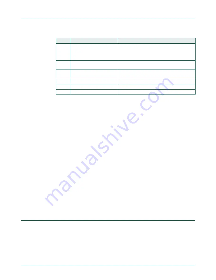
Table 276. ADC hardware trigger inputs
Input #
Source
Description
0
-
This source is always a logic HIGH. Use this trigger
source when running the ADC without hardware
triggers or when using a software trigger to avoid
spurious conversion triggers.
1
ADC_PINTRG0
ADC pin trigger 0. Connect to an external pin through
the switch matrix.
2
ADC_PINTRIG1
ADC pin trigger 1. Connect to an external pin through
the switch matrix.
3
SCT0_OUT3
SCT output 3.
4
ACMP_O
Analog comparator output.
5
ARM_TXEV
ARM core TXEV event.