NXP Semiconductors KITVR5510 A0EVM Series Скачать руководство пользователя страница 16

NXP Semiconductors

UM11587

KITVR5510xA0EVM Evaluation Kit User Guideline
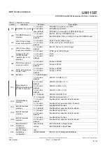
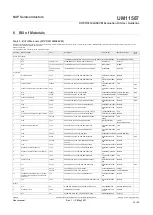
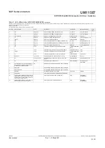
6 Bill of Materials

NXP does not assume liability, endorse, or warrant components from external manufacturers that are referenced in circuit drawings or tables. While NXP offers component recommendations in this configuration, it is the

customer’s responsibility to validate their application.
DNP: do not populate
For critical components, it is vital to use the manufacturer listed.

Quantity

Schematic label

Value

Description

Part number

Manufacturer name

Assy

Opt

Active components

1

U15

IC PWR MANAGEMENT QM -0.3/5.5 V 60 V AEC-Q100 QFN56 MVR5510AMMA0ES

NXP SEMICONDUCTORS

1

U16

250 mW, 7.5 V

DIODE ZENER 7.5 V 250 mW AEC-Q101 SOT23

BZX84-A7V5

Nexperia

1

U17

1.5-15 V 150 mA 2.5-16

V

IC LIN VREG LDO 1.5-15 V 150 mA 2.5-16 V SOT23-5

MIC5205YM5

MICREL

1

U20

1.25 V-60 V 50 mA

4.5-60 V

IC LIN VREG ADJ 1.25 V-60 V 50 mA 4.5-60 V SOP-8

RT9068GSP

RICHTEK

Capacitors

4

C11,C15,C24,C25

22 μF

CAP CER 22 μF 10 V 10% X7R AEC-Q200 1206

GCM31CR71A226KE

02

MURATA

1

C115

47 μF

CAP CER 47 μF 10 V 20% X5R AEC-Q200 1206

GRT31CR61A476ME

13L

MURATA

3

C121,C122,C123

1000 pF

CAP CER 1000 pF 50 V 10% X7R AEC-Q200 0603

CGA3E2X7R1H102K

080AA

TDK

DNP

8

C124,C125,C126,C127,C128,C129,C130,C131 22 μF

CAP CER 22 μF 10 V 10% X7R AEC-Q200 1206

GCM31CR71A226KE

02

MURATA

DNP

1

C13

2200 pF

CAP CER 2200 pF 50 V 10% X7R 0603

C0603X7R500-222KNE VENKEL COMPANY

DNP

1

C132

470 pF

CAP CER 470 pF 50 V 5% C0G 0603

CC0603JRNPO9BN471 YAGEO AMERICA
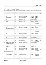
4

C133,C134,C135,C136

22 pF

CAP CER 22 pF 50 V 1% C0G 0402

04025A220FAT2A

AVX

DNP

1

C14

1000 pF

CAP CER 1000 pF 50 V 10% X7R AEC-Q200 0402

GCM155R71H102KA

37D

MURATA

DNP

1

C153

4.7 μF

CAP CER 4.7 μF 10 V 10% X7S AEC-Q200 0805

GCM21BC71A475KA73 MURATA

2

C155,C174

1.0 μF

CAP CER 1.0 μF 16 V 10% X6S 0402

GRM155C81C105KE

11D

MURATA

1

C156

2.2 μF

CAP TANT ESR=1.800 ΩS 2.2 μF 10 V 10% 3216-18

TPSA225K010R1800

AVX

9

C16,C17,C26,C66,C67,C94,C102,C176,C177

0.1 μF

CAP CER 0.1 μF 50 V 10% X7R AEC-Q200 0402

GCM155R71H104KE02 MURATA

1

C162

0.047 μF

CAP CER 0.047 μF 50 V 10% X7R AEC-Q200 0603

CGA3E2X7R1H473K

080AA

TDK

1

C163

47 μF

CAP ALEL 47 μF 50 V 20% AEC-Q200 SMD

MAL214699101E3

VISHAY

INTERTECHNOLOGY

5

C164,C165,C166,C167,C168

10 μF

CAP CER 10 μF 50 V 10% X7S AEC-Q200 1210

CGA6P3X7S1H106K2

50AB

TDK

1

C172

1 μF

CAP CER 1 μF 25 V 10% X7R AEC-Q200 0603

CGA3E1X7R1E105K0

80AC

TDK

1

C173

0.22 μF

CAP CER 0.22 μF 50 V 10% X7R 0805

C0805X7R500-224KNE VENKEL COMPANY

1

C178

330 pF

CAP CER 330 pF 50 V 5% C0G AEC-Q200 0402

GCM1555C1H331JA

16D

MURATA

DNP

2

C179,C180

0.022 μF

CAP CER 0.022 μF 50 V 10% X7R AEC-Q200 0402
0.022 μF

GCM155R71H223KA

55D

MURATA

1

C181

18 pF

CAP CER 18 pF 50 V 5% C0G AEC-Q200 0402

GCM1555C1H180JA16 MURATA

6

C19,C23,C104,C105,C108,C110

4.7 μF

CAP CER 4.7 μF 16 V 10% X7R AEC-Q200 0805

GCM21BR71C475KA

73

MURATA

8

C20,C21,C106,C107,C148,C149,C150,C161

22 uF

CAP CER 22 uF 16 V 20% X7R AEC-Q200 1210

GCM32ER71C226ME

19

MURATA

1

C61

10 μF

CAP CER 10 μF 16 V 20% X7S AEC-Q200 0805

CGA4J1X7S1C106M1

25AC

TDK

3

C69,C113,C154

1000 pF

CAP CER 1000 pF 50 V 10% X7R AEC-Q200 0402

GCM155R71H102KA

37D

MURATA

1

C71

0.01 μF

CAP CER 0.01 μF 50 V 10% X7R AEC-Q200 0402

GCM155R71H103KA

55D

MURATA

DNP

1

C72

0.01 μF

CAP CER 0.01 μF 50 V 5% X7R 0603

C0603C103J5RACTU

KEMET

1

C76

0.022 μF

CAP CER 0.022 μF 25 V 10% X7R 0603

CC0603KRX7R8BB223 YAGEO AMERICA

17

C95,C96,C97,C98,C100,C112,C137,C138,C1

39,C140,C141,C142,C143,C144,C145,C146,

C147,C160

1 μF

CAP CER 1 μF 10 V 10% X7S AEC-Q200 0402

GCM155C71A105KE

38D

MURATA

1

C99

1.0 μF

CAP CER 1.0 μF 50 V 10% X7R FAIL SAFE AEC-Q200 1206

GCJ31CR71H105KA

12L

MURATA

Diodes

1

D10

2 A

DIODE SCH PWR RECT 2 A 60V AEC-Q101 SOD-123

NRVTS260ESFT1G

ON SEMICONDUCTOR

4

D12,D13,D14,D15

20 mA

LED RED SGL 20 mA SMT

LS M67K-H2L1-1-0-2-

R18-Z

OSRAM

1

D27

5 A

DIODE SCH RECT 60 V 5 A AEC-Q101 SOT1289

PMEG060V050EPD

Nexperia

Table 3. Bill of Materials (KITVR5510MA0EVM)

UM11587

All information provided in this document is subject to legal disclaimers.

© NXP B.V. 2021. All rights reserved.

User manual

Rev. 1 — 3 May 2021

16 / 32

Содержание KITVR5510 A0EVM Series

Страница 1: ...Keywords VR5510 KITVR5510xA0EVM evaluation kit automotive multi output power management integrated circuit Abstract This user manual describes how to use the KITVR5510xA0EVM evaluation kit The VR5510...

Страница 2: ...Kit User Guideline Rev Date Description v 1 20210503 Initial version Modifications NA Revision history UM11587 All information provided in this document is subject to legal disclaimers NXP B V 2021 A...

Страница 3: ...in the evaluation design implementation and validation of VR5510 Power Management Integrated Circuit PMIC for high performance applications The scope of this document is to provide the user with info...

Страница 4: ...and tools parametrics ordering information and a Getting Started tab The Getting Started tab provides quick reference information applicable to using the KITVR5510xA0EVM evaluation board including the...

Страница 5: ...5 0 V to 24 0 V and current limit set initially to 100 mA Two power supply cables with banana connectors at one end 3 3 Windows PC workstation This evaluation board requires a Windows PC workstation...

Страница 6: ...evice The KITVR5510xA0EVM includes NXPs FRDM K82F development platform board The FRDM K82F attaches to the bottom of the board and serves as the communication interface between the KITVR5510xA0EVM and...

Страница 7: ...eleased D6 Green RSTB_G External RSTB signal RSTB released D12 Red RSTB_R External RSTB signal RSTB asserted low D13 Red PGOOD_R External PGOOD signal PGOOD asserted low D14 Red INTB External INTB sig...

Страница 8: ...Figure 2 Connectors Figure 2 shows all of the connectors on the KITVR5510xA0EVM Pinouts for individual connectors are shown in the schematic UM11587 All information provided in this document is subjec...

Страница 9: ...11 Debug mode selection 2 3 shorted default GND to normal mode 1 2 shorted 7P5V generated from VBAT VIN directly J12 Debug mode selection 2 3 shorted default 7P5V generated from an onboard regulator 1...

Страница 10: ...default open 1 2 shorted default VMON1 VPRE 3 3 V 3 4 shorted default VMON2 BUCK3 1 1 V 5 6 shorted default VMON3 LDO2 1 8 V 7 8 shorted default VMON4 LDO1 1 8 V 9 10 shorted VMON4 BOOST 5 V J101 Regx...

Страница 11: ...horted default BUCK2 in both Single and Multiphase Table 2 Jumpers continued 4 3 4 Test points Figure 4 shows the location and the function of the test points on the KITVR5510xA0EVM board Figure 4 Tes...

Страница 12: ...Kit User Guideline 5 Layout Figure 5 KITVR5510xA0EVM layout top Figure 6 KITVR5510xA0EVM layout layer 2 UM11587 All information provided in this document is subject to legal disclaimers NXP B V 2021 A...

Страница 13: ...ion Kit User Guideline Figure 7 KITVR5510xA0EVM layout layer 3 Figure 8 VR551 xA0EVM layout layer 4 UM11587 All information provided in this document is subject to legal disclaimers NXP B V 2021 All r...

Страница 14: ...n Kit User Guideline Figure 9 KITVR5510xA0EVM layout layer 5 Figure 10 KITVR5510xA0EVM layout layer 6 UM11587 All information provided in this document is subject to legal disclaimers NXP B V 2021 All...

Страница 15: ...n Kit User Guideline Figure 11 KITVR5510xA0EVM layout layer 7 Figure 12 KITVR5510xA0EVM layout bottom UM11587 All information provided in this document is subject to legal disclaimers NXP B V 2021 All...

Страница 16: ...26 C66 C67 C94 C102 C176 C177 0 1 F CAP CER 0 1 F 50 V 10 X7R AEC Q200 0402 GCM155R71H104KE02 MURATA 1 C162 0 047 F CAP CER 0 047 F 50 V 10 X7R AEC Q200 0603 CGA3E2X7R1H473K 080AA TDK 1 C163 47 F CAP...

Страница 17: ...02 RK73H1ETTP6203F KOA SPEER 1 R252 115 K RES MF 115 K 1 10 W 1 AEC Q200 0402 RK73H1ETTP1153F KOA SPEER 1 R258 1 00 K RES MF 1 00 K 1 10 W 0 1 AEC Q200 0603 ERA3AEB102V PANASONIC 1 R259 10 K RES MF 10...

Страница 18: ...1 0 H IND PWR 1 0 H 100KHz 17 9A 20 AEC Q200 SMD SPM6545VT 1R0M D TDK 3 L4 L5 L6 1 0 H IND PWR 1 0 H 1 MHZ 4 7A 20 AEC Q200 SMD TFM252012ALMA1R0 MTAA TDK 1 L7 4 7 H IND PWR 4 7 H 100 kHz 11A 20 AEC Q2...

Страница 19: ...m board 3 Drag and drop the downloaded file 0244_k20dx_bootloader_update_0x8000 bin into the BOOTLOADER drive Note Ensure that enough time is allowed for the firmware to be saved in the boot loader 4...

Страница 20: ...ry DAPLink bootloader update 4 Disable the storage services Run services msc then double click on the storage service from the list and press the stop button 5 Press the RST push button on the Freedom...

Страница 21: ...ot available during the development phase the following steps can be taken to operate the PMIC in different modes 1 If the FRDM K82F board must be programmed or if the firmware must be flashed again f...

Страница 22: ...ating with VR5510 on the reference board follow the steps in Section 7 3 Connecting to the KITVR5510xA0EVM board Figure 14 Connecting to a reference board with K82F only UM11587 All information provid...

Страница 23: ...the NXPGUI tool 1 To open the OTP configuration tool click the OTP icon on the left side of the NXPGUI The OTP tool can be used independently of the EV kit board status the board does not have to be...

Страница 24: ...be in position 2 ON Set SW2 to ON position enables the debug mode of operation Turns on the part in debug mode 6 When the PMIC is ON verify the debug mode of operation by reading the FS_STATES 0x18 re...

Страница 25: ...follow the steps mentioned in Section 8 1 Operating in debug mode An OTP script can be created using the OTP section of the tool as explained above in Section 8 1 Operating in debug mode 1 Follow step...

Страница 26: ...ramming separately then select the target state machine and click the program button Follow the instructions 7 If the OTP fuse burning was successful the progress is updated and the fuse box status is...

Страница 27: ...User Guideline burning power cycle the board and check if the part turns on with the expected configuration UM11587 All information provided in this document is subject to legal disclaimers NXP B V 20...

Страница 28: ...pdf VR5510 Data sheet VR5510 Multi Output PMIC with SMPS and LDO data sheet https www nxp com docs en data sheet VR5510 pdf VR5510 Safety Manual VR5510 Multi Output PMIC with SMPS and LDO Safety manua...

Страница 29: ...customer s third party customer s NXP does not accept any liability in this respect Terms and conditions of commercial sale NXP Semiconductors products are sold subject to the general terms and condi...

Страница 30: ...r Guideline Tables Tab 1 LEDs 7 Tab 2 Jumpers 9 Tab 3 Bill of Materials KITVR5510MA0EVM 16 Tab 4 References 28 UM11587 All information provided in this document is subject to legal disclaimers NXP B V...

Страница 31: ...14 Fig 11 KITVR5510xA0EVM layout layer 7 15 Fig 12 KITVR5510xA0EVM layout bottom 15 Fig 13 Freedom board 19 Fig 14 Connecting to a reference board with K82F only 22 Fig 15 NXP GUI OTP configuration t...

Страница 32: ...ring Software and Tools 19 7 1 Freedom board BOOTLOADER refresh in a Windows 7 system 19 7 2 Freedom Board BOOTLOADER Refresh in a Windows 10 System 20 7 3 Connecting to the KITVR5510xA0EVM board 21 7...

Отзывы: