


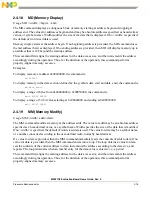


M5251C3 Evaluation Board Users Guide, Rev. 0
3-2
Freescale Semiconductor
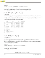
points to the Flash memory. The contents of the exception table are written to address $00000000 in the
SDRAM. The Software Watchdog Timer is disabled, the Bus Monitor is enabled, and the internal timers
are placed in a stop condition. The interrupt controller registers are initialized with unique interrupt
level/priority pairs. A memory map for the entire board can be seen in
3.1.3
HIZ Signal
The assertion of the -HIZ signal forces all output drivers to a high-impedance state. On the M5251C3
board the high impedance signal is pulled to +3.3V via a 4.7K pull-up resistor, ensuring that the output
drivers will not be in a high-impedance state during reset.
3.1.4
Clock Circuitry
The M5251C3 board uses a 11.2896MHz crystal (X2 on the schematics) to provide the clock to the
processor (IC1). In addition to the 11.2896MHz crystal, there is also a 24MHz crystal (X4) which feeds
the USB section of IC1, a 32.768KHz crystal (X3) which feeds the RTC section of IC1 and a second
11.2896 MHz crystal (X1) that can be used to provide an external audio clock source
3.1.5
Watchdog Timer
The duration of the Watchdog is selected by the SWT[1:0] bits in the System Protection and Control
Register (SYPCR), SWT[1:0] = 11 gives a maximum timeout period of 2
28
/System frequency. The dBUG
monitor initializes these bits with the value 0x11, which provides the maximum time-out period, but dBUG
does
NOT
enable the watchdog timer via the SYPCR register SWE bit.
3.1.6
Interrupt Sources
The ColdFire® family of processors can receive seven levels of interrupt priorities. When the processor
receives an interrupt which has a higher priority than the current interrupt mask (in the status register), it
will perform an interrupt acknowledge cycle at the end of the current instruction cycle. This interrupt
acknowledge cycle indicates to the source of the interrupt that the request is being acknowledged and the
device should provide the proper vector number to indicate where the service routine for this interrupt level
is located. If the source of interrupt is not capable of providing a vector, its interrupt should be set up as an
autovector interrupt which directs the processor to a predefined entry in the exception table. (See the
MCF5251 Reference Manual
).
The processor goes to an exception routine via the exception table. This table is stored in the Flash
EEPROM. The address of the table location is stored in the VBR. The dBUG ROM monitor writes a copy
of the exception table into the RAM starting at $00000000. To set an exception vector, the user places the
address of the exception handler in the appropriate vector in the vector table located at $00000000 and then
points the VBR to $00000000.
The MCF5251 microprocessor has seven external interrupt request lines -INT[6:0], all of which are
multiplexed with other functions. The interrupt controller is capable of providing up to 75 interrupt
sources. These sources include:-
•
External interrupt signals -INT[6:0]
Содержание freescale M5251C3
Страница 1: ...Document Number M5251C3UG Rev 0 05 2006 M5251C3 Evaluation Board Users Guide ...
Страница 6: ...M5251C3 Evaluation Board Users Guide Rev 0 vi Freescale Semiconductor ...
Страница 14: ...M5251C3 Evaluation Board Users Guide Rev 0 1 8 Freescale Semiconductor Figure 1 4 Default Jumper Locations ...
Страница 18: ...M5251C3 Evaluation Board Users Guide Rev 0 1 12 Freescale Semiconductor ...
Страница 42: ...M5251C3 Evaluation Board Users Guide Rev 0 2 24 Freescale Semiconductor ...
Страница 68: ...M5251C3 Evaluation Board Users Guide Rev 0 B 6 Freescale Semiconductor ...