


AN11001
All information provided in this document is subject to legal disclaimers.
© NXP B.V. 2011. All rights reserved.
Application note
Rev. 1 — 7 March 2011
8 of 17
NXP Semiconductors
AN11001
CBTL02042A switching application for mSATA, PCIe Mini-Card
4.2 SATA routing guideline (without multiplexer in topology)
General routing and placement guidelines for SATA signals are:
•
SATA signals should be referenced to internal ground plane. If it is necessary to
change reference to power plane (such that SATA signals are routed on the bottom
layer, which is referenced to power or V
CC
plane on PCB), capacitors with low ESR
values should be placed at locations where the SATA signals are changing layers,
and between power and ground planes to minimize the negative impact of EMI and
signal integrity performance caused by reference plane change. These capacitors
provide a high frequency current return path between different reference planes, and
minimize the impedance discontinuity and current loop area that crossing different
reference planes created.
•
Route differential traces over a continuous ground planes with no interruptions.
Routing across a split ground plane (which contains anti-etch) should be avoided.
•
If a layer change is absolutely necessary, make sure the trace matching for either
transmit or receive pair occurs within the same layer. It is also recommended to not to
use vias whenever possible. A maximum of four vias are allowed on the path,
inclusive of the though-hole via of the external connector.
•
Route TX and RX pairs close to each other and on the same PCB layer with minimum
mismatch of trace length within the pair. Trace length matching should be within the
differential pair for each segment between points of discontinuity. Points of
discontinuity could be vias, capacitor pads, or connector pins. Total length mismatch
should not exceed 20 mils. It is not necessary to match the trace length of TX and RX
pairs since they operate independently.
•
Do not route SATA traces under power connectors, other interface connectors,
crystals, oscillators, clock synthesizers, or magnetic devices that use and/or duplicate
clocks.
•
Route SATA signal traces away from etching areas, including pads, vias, and other
signal traces. Keep minimum keep-out distance of 20 mils whenever possible.
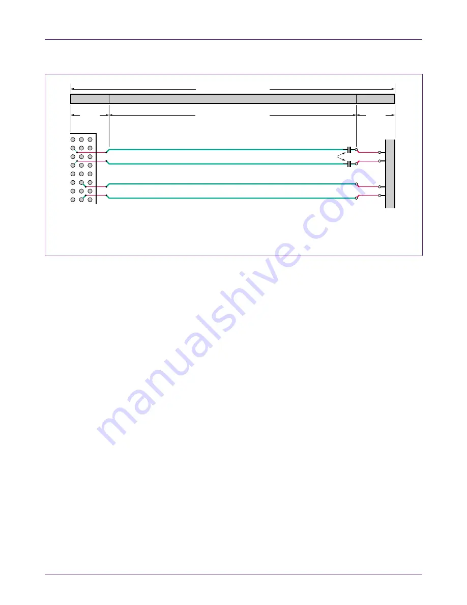
Locations of vias and routing layer changes shown in this figure are for illustration purposes only. PCB layout design should
minimize the use of vias and layer changes during routing process as discussed in the general guideline.
Fig 4.
Mini-Card topology example
BREAKOUT
maximum
500 mil
(0.5 inch;
1.27 cm)
MAIN ROUTE
maximum 20.32 cm (8 inches)
BREAKOUT
500 mil
maximum 25.4 cm (10 inches)
PETp0
PETn0
PERp0
PERn0
MiniCard connector
72 nF to 200 nF
019aaa990