N58 Hardware User Guide
Chapter 5 Application Interfaces
Copyright © Neoway Technology Co., Ltd. All rights reserved.
65
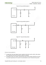
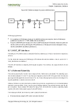
capacitance less than 0.5 pF. Ensure that the reverse breakdown voltage of the TVS diode is
greater than 10 V (above 15 V is recommended).
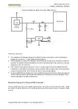
PCB design guidelines:
Lay the ground copper foil around the RF cable. Evenly dig as many ground holes as possible
on the ground copper foil, and control the trace impedance to 50 Ω.
The PCB trace between the module RF pin and RF cable should be as short as possible. Control
the trace impedance to 50 Ω.
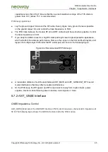
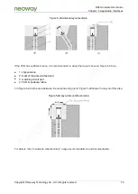
If you adopt an SMA connector, a big RF solder pad might result in great parasitic capacitance,
which will affect the antenna performance. Remove the copper on the first and fourth layers or all
layers of a multiple-layer PCB under the RF solder pad, as shown in the following figure.
Figure 5-42 Recommended RF PCB design
A reasonable distance should be kept between ANT_MAIN and ANT_GNSS/ANT_BT to avoid
mutual interference that may affect reception performance.
On the PCB, keep the RF signals and RF components far away from digital circuits, power
supplies, electronic transformers, power inductors, clock signals, or more.
5.7.2 ANT_GNSS Interface
GNSS Impedance Control
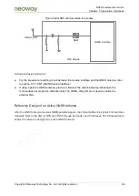
ANT_GNSS (92nd pin) is the GNSS RF interface of N58, which requires a characteristic impedance of
50 Ω. The following figure shows the GNSS structure inside the N58 module.

