


N58 Hardware User Guide
Chapter 5 Application Interfaces
Copyright © Neoway Technology Co., Ltd. All rights reserved.
50
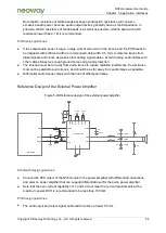
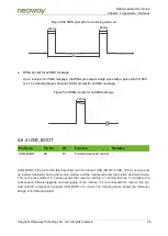
Schematic design guidelines:
The VDD_SDCPULL power supply is the 1.8 V/3.0 V dual-voltage and is configured by software
based on the SD card voltage type. The maximum output current of VDD_SDCPULL is 150 mA,
and VDD_SDCPULL is used only for the pull-up power supply of the SD card data cable and
CMD. Do not use VDD_SDCPULL for other purposes.
The recommended voltage at the power supply for the SD card ranges from 2.85 V to 3.2 V
(typical value: 3 V), and the current is greater than 500 mA. The voltage is generated by an LDO
or DC-DC circuit.
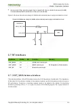
SD card insertion/removal detection is related to the structure of the SD card connector. Its
principle is that the SDC_DET pin levels are inverted before and after an SD card is inserted,
triggering interruption. You can choose to configure the effective level of insertion detection as
high or low level by using software based on the structure of the card connector.
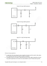
PCB design guidelines:
The trace of the power supply cable must be wider than 0.5 mm.
The trace lengths of SDIO cables must be the same. The length difference between DATA
cables must be less than 0.5 mm, and that between CMD, CLK, and DATA cables must be less
than 0.5 mm.
The distance between DATA cables must be greater than 2 times the cable width.
Control the impedance for
each signal cable connected to the SDIO interface to 50 Ω.
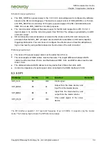
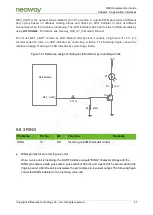
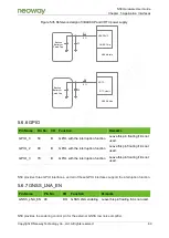
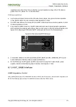
5.3.5 SPI
Pin Name
Pin No.
I/O
Function
Remarks
SPI_CLK
84
DO
Clock signal
-
SPI_MISO
85
B
Output from the slave device, and
input from the master device
-
SPI_MOSI
86
B
Input from the slave device, and
output from the master device
-
SPI_CS_N
87
DO
Chip select signal of the slave
device
-
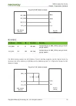
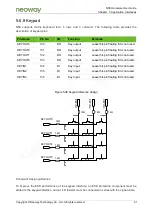
The SPI interface supports 1.8 V level and frequency of up to 50 MHz. It supports only the master
mode. The following figure shows the
SPI
reference design.