602
Chapter 14
A/D Converter
User’s Manual U16580EE3V1UD00
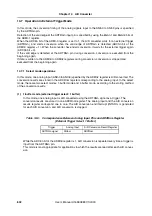
14.7 Operation in External Trigger Mode
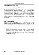
In this mode, the conversion timing of the analog signals input to the ANIn0 to ANIn9 pins is specified
by the ADTRGn pin.
Detection of the valid edge at the ADTRGn input pin is specified by using the EGAn1 and EGAn0 bits of
the ADMn1 register.
When the ADCEn bit of the ADMn0 register is set to 1, the A/D converter waits for an external trigger
(ADTRGn), and starts conversion when the valid edge of ADTRGn is detected (ADCSn bit of the
ADMn0 register = 1). When the converter has ended conversion, it waits for the external trigger again
(ADCSn bit = 0).
If the valid edge is detected at the ADTRGn pin during conversion, conversion is executed from the
beginning again.
If data is written to the ADMn0 to ADMn2 registers during conversion, conversion is stopped and
executed from the beginning again.
14.7.1 Select mode operations
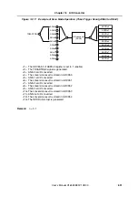
In this mode, one analog input (ANIn0 to ANIn9) specified by the ADMn2 register is A/D converted. The
conversion results are stored in the ADCRnm register corresponding to the analog input. In the select
mode, there are two select modes: 1-buffer mode and 4-buffer mode, according to the storing method
of the conversion results.
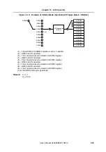
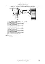
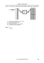
(1)
1-buffer mode (external trigger select: 1 buffer)
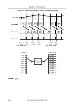
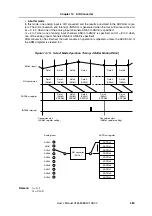
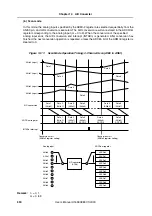
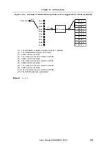
In this mode, one analog input is A/D converted using the ADTRGn signal as a trigger. The
conversion results are stored in one ADCRnm register. The analog input and the A/D conversion
results register correspond one to one. The A/D conversion end interrupt (INTADn) is generated
for each A/D conversion, and A/D conversion is stopped.
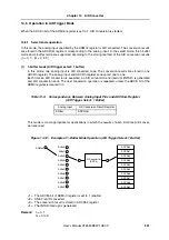
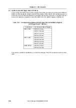
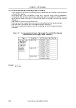
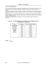
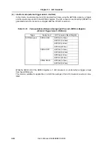
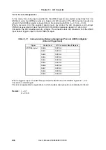
Table 14-9:
Correspondence Between Analog Input Pins and ADCRnm Register
(External Trigger Select: 1 Buffer)
While the ADCEn bit of the ADMn0 register is 1, A/D conversion is repeated every time a trigger is
input from the ADTRGn pin.
This mode is most appropriate for applications in which the results are read after each A/D conver-
sion.
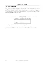
Trigger
Analog Input
A/D Conversion Result Register
ADTRGn signal
ANInm
ADCRnm
Содержание V850E/PH2
Страница 6: ...6 Preface User s Manual U16580EE3V1UD00...
Страница 16: ...16 User s Manual U16580EE3V1UD00...
Страница 28: ...28 User s Manual U16580EE3V1UD00...
Страница 32: ...32 User s Manual U16580EE3V1UD00...
Страница 84: ...84 Chapter 2 Pin Functions User s Manual U16580EE3V1UD00 MEMO...
Страница 144: ...144 Chapter 3 CPU Functions User s Manual U16580EE3V1UD00 MEMO...
Страница 192: ...192 Chapter 5 Memory Access Control Function PD70F3187 only User s Manual U16580EE3V1UD00 MEMO...
Страница 312: ...312 Chapter 9 16 Bit Timer Event Counter P User s Manual U16580EE3V1UD00 MEMO...
Страница 534: ...534 Chapter 11 16 bit Timer Event Counter T User s Manual U16580EE3V1UD00...
Страница 969: ...969 Chapter 20 Port Functions User s Manual U16580EE3V1UD00 MEMO...
Страница 970: ...970 Chapter 20 Port Functions User s Manual U16580EE3V1UD00...
Страница 976: ...976 Chapter 22 Internal RAM Parity Check Function User s Manual U16580EE3V1UD00 MEMO...
Страница 984: ...984 Chapter 23 On Chip Debug Function OCD User s Manual U16580EE3V1UD00 MEMO...
Страница 1006: ...1006 Chapter 24 Flash Memory User s Manual U16580EE3V1UD00 MEMO...
Страница 1036: ...1036 Chapter 27 Recommended Soldering Conditions User s Manual U16580EE3V1UD00 MEMO...
Страница 1046: ...1046 Appendix A Index User s Manual U16580EE3V1UD00 MEMO...
Страница 1052: ...1052 User s Manual U16580EE3V1UD00...
Страница 1053: ......

