background image

LM48821 Evaluation Board
User's Guide

National Semiconductor
Application Note 1589
Kevin Hoskins
May 2007

Quick Start Guide

Connect the I

2

C signal generation and interface board to a

computer’s parallel port.
Install LM48821 control software: “LM48821_Software.”
Amplifier output mode:
Apply a 2.0V to 4.0V power supply’s positive voltage output
to the “VDD” pin on jumper J6. Apply the power supply’s
ground return to the “GND“ pin on J6.
Connect the supplied 5-wire cable between the I

2

C signal

generation and interface board and the 5-pin connector (I2C
Interface) on the LM48821 demonstration board.
Apply a stereo audio signal to jumpers JP2(Left) and JP3
(Right). Apply the source’s +input and -input to the “+” pin and
the “-“ pin, respectively.
Connect a load (

 16Ω

) to JP(Right) and another load to JP5

(Left). JP4’s “+” pin and JP’s “+” pin carries the output signals

from the two amplifiers found on pins OUTR and OUTL, re-
spectively.
Apply power. Make measurements. Plug in a pair of head-
phones. Enjoy.

Introduction

To help the user investigate and evaluate the LM48821's per-
formance and capabilities, a fully populated demonstration
board is available from the National Semiconductor
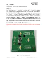
Corporation's Audio Products Group. This board is shown in
Figure 1. Connected to an external power supply (2.0V to
4.0V), a signal source and an I

2

C controller (or signal source),

the LM48821 demonstration board easily demonstrate the
amplifier's features.

30009811

FIGURE 1. The LM48821 Demonstration Board

© 2007 National Semiconductor Corporation

300098

www.national.com

LM48821 Evaluation Board User's Guide

AN-1589

Содержание LM48821

Страница 1: ...and input to the pin and the pin respectively Connect a load 16Ω to JP Right and another load to JP5 Left JP4 s pin and JP s pin carries the output signals from the two amplifiers found on pins OUTR and OUTL re spectively Apply power Make measurements Plug in a pair of head phones Enjoy Introduction To help the user investigate and evaluate the LM48821 s per formance and capabilities a fully popul...

Страница 2: ...r battery powered potable systems The LM48821 includes separate shutdown controls for each stereo channel for micropower dissipation an internal thermal shutdown protection mechanism and is unity gain stable Operating Conditions Temperature Range 40 C TA 85 C Amplifier Power Supply Voltage 2 0V VDD 5 0V 4 0V Board Features The LM48821 demonstration board has all of the necessary connections using ...

Страница 3: ...sponds to the headphone jack s ring connection J4 s pin labeled R OUT corresponds to the headphone jack s sleeve or ground connection J5 This is the connection to the amplifier s single ended ground referenced left channel output Connect the J5 pin labeled L OUT and the pin labeled L OUT to the positive and ground inputs respectively of an external signal measurement device J5 s pin labeled L OUT ...

Страница 4: ...e program s window Each time the slider is moved from one tick mark to another the program updates the amplifier s volume control LEFT CHANNEL BOTH CHANNELS and RIGHT CHAN NEL controls each have two buttons For the left and right channel control the ON button activates its respective chan nel whereas the OFF button places its respective channel in shutdown mode Selecting the BOTH CHANNELS ON butto...

Страница 5: ...5R1A104M C6 C8 Multilayer Ceramic Capacitor 4 7μF 20 6 3V 0603 TDK C1608X5R1A475M C7 Multilayer Ceramic Capacitor 4 7μF 20 10V 0805 TDK C2012X5R1A475M J1 Headphone Jack J2 J6 2 pin header 100mil lead pitch J8 5 pin header 100mil lead pitch JU1 3 pin header 100mil lead pitch U1 LM48821Direct Coupled Tru GND Ultra Low Noise 80mW Differential Inputs Stereo Headphone Amplifier with I2C Volume Control ...

Страница 6: ... parts location Figure 5 is the top layer Figure 6 is the upper inner layer Figure 7 is the lower middle layer Figure 8 is the bottom layer Figure 9 is the bottom silkscreen layer 30009845 Figure 4 Top Silkscreen Shown 2 6X actual size 30009844 Figure 5 Top Layer Shown 2 6X actual size 30009842 Figure 6 Upper Middle Layer Shown 2 6X actual size www national com 6 AN 1589 ...

Страница 7: ...30009843 Figure 7 Lower Middle Layer Shown 2 6X actual size 30009840 Figure 8 Bottom Layer Shown 2 6X actual size 30009841 Figure 9 Bottom Silk Layer Shown 2 6X actual size 7 www national com AN 1589 ...

Страница 8: ...at from left to right at 1 THD N VDD 2V VDD 3V VDD 4V both channels driven and measured 30009853 Stereo THD N vs Output Power RL 16Ω AV 0dB f 10kHz at from left to right at 1 THD N VDD 2V VDD 3V VDD 4V both channels driven and measured 30009854 Stereo THD N vs Output Power RL 32Ω AV 0dB f 100Hz at from left to right at 1 THD N VDD 2V VDD 3V VDD 4V both channels driven and measured 30009858 www nat...

Страница 9: ...THD N VDD 2V VDD 3V VDD 4V both channels driven and measured 30009857 Stereo THD N vs Frequency RL 16Ω AV 0dB at from left to bottom at 10kHz VDD 2V POUT 7mW VDD 3V POUT 36mW VDD 4V POUT 92mW both channels driven and measured 30009851 Stereo THD N vs Frequency RL 32Ω AV 0dB at from left to bottom at 10kHz VDD 2V POUT 10mW VDD 3V POUT 38mW VDD 4V POUT 85mW both channels driven and measured 30009852...

Страница 10: ...ented by manipulating the bits within the internal I2C control register Table A1 LM48821 I2C Control Register Addressing and Data Format Chart D7 D6 D5 D4 D3 D2 D1 D0 I2C Address 1 1 1 0 1 1 0 0 Control Register V4 V3 V2 V1 V0 MUTE LEFT ENABLE RIGHT ENABLE www national com 10 AN 1589 ...

Страница 11: ... control settings Table B1 Binary Values for the Different Volume Control Gain Settings Gain B4 B3 B2 B1 B0 18 1 1 1 1 1 17 1 1 1 1 0 16 1 1 1 0 1 15 1 1 1 0 0 14 1 1 0 1 1 13 1 1 0 1 0 12 1 1 0 0 1 10 1 1 0 0 0 8 1 0 1 1 1 6 1 0 1 1 0 4 1 0 1 0 1 2 1 0 1 0 0 0 1 0 0 1 1 2 1 0 0 1 0 4 1 0 0 0 1 6 1 0 0 0 0 8 0 1 1 1 1 10 0 1 1 1 0 12 0 1 1 0 1 14 0 1 1 0 0 16 0 1 0 1 1 18 0 1 0 1 0 21 0 1 0 0 1 24...

Страница 12: ...re information on Micro SMD Wafer Level Chip Scale Package Since National Semiconductor is constantly pursuing the best package performance possible please refer to the following web page for possible updates to the μSMD package infor mation presented in Appendix D http www national com an AN AN 1112 pdf www national com 12 AN 1589 ...

Страница 13: ...Revision History Rev Date Description 1 0 05 14 07 Initial release 13 www national com AN 1589 ...

Страница 14: ...RTY RIGHT LIFE SUPPORT POLICY NATIONAL S PRODUCTS ARE NOT AUTHORIZED FOR USE AS CRITICAL COMPONENTS IN LIFE SUPPORT DEVICES OR SYSTEMS WITHOUT THE EXPRESS PRIOR WRITTEN APPROVAL OF THE CHIEF EXECUTIVE OFFICER AND GENERAL COUNSEL OF NATIONAL SEMICONDUCTOR CORPORATION As used herein Life support devices or systems are devices which a are intended for surgical implant into the body or b support or su...

Отзывы: