Chapter 3
Theory of Operation
© National Instruments Corporation
3-13
SCXI-1100 User Manual
for each gain you use to eliminate error caused by drift in the PGIA internal circuitry and to
increase the accuracy of the measurement. After you determine the offset, you can determine the
analog input as follows:
V
in
= (V
out
- V
ofs
)/G
PGIA
where V
in
is the analog input voltage, G
PGIA
is the PGIA gain, V
out
is the SCXI-1100 output,
and V
ofs
is the measured offset voltage at the gain G
PGIA
.
Notice that the auto-zero path is different from the analog input path; therefore, even after auto-
zeroing, a residual input offset still exists and has a value of less than 5
µ
V.
Inherently, the SCXI-1100 offsets and gain errors are small, as shown in Appendix A,
Specifications; therefore, hardware calibration is not necessary and the software calibration
procedure explained in the previous paragraph is adequate.
Analog Output Circuitry
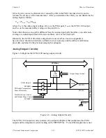
Figure 3-8 diagrams the SCXI-1100 analog output circuitry.
PGIA Output
>>
MTEMP
PGIA and Temperature
Sensor Reference
>>
DTEMP
To
AB0
Switch
SCXIbus
Buffer
MCH0-
MCH1+
Rear
Signal Connector
Output Stage Control
MCH1-
Hardware Scan Control
and Output Stage Control
MCH0+
Figure 3-8. Analog Output Circuitry
The SCXI-1100 output circuitry consists of an output multiplexer that multiplexes the PGIA
output and the temperature sensor reading on the MTEMP line. To read the temperature sensor


