background image

Chapter 3

Theory of Operation

© National Instruments Corporation

3-9

SCXI-1100 User Manual

When you reset the SCXIbus, all bits in the Configuration Register clear.

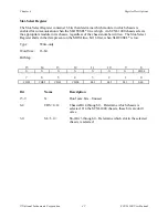
The Module ID Register connects to MISO on the SCXIbus.  The Module ID Register is an 8-bit
parallel/serial-in serial-out shift register and an SPI communication adapter.  During the first four
bytes of transfer after SS* is asserted low, the contents of the Module ID Register are written
onto MISO.  Zeros are written to MISO thereafter until SS* is released and reasserted.  The
SCXI-1100 module ID is hex 00000006.

Analog and Timing Circuitry

The SCXIbus produces analog power (

±

18.5 VDC) that is regulated on the SCXI-1100 to

±

15 VDC, a guard, analog buses (AB0

±

, AB2

±

) and a chassis ground (CHSGND).  AB0

±

 buses

the SCXI-1100 output to other modules or receives outputs from other modules via the SCXIbus.
The module can use AB2

±

 to receive a precision voltage for auto calibration of the PGIA.  Refer

to the Calibration section later in this chapter for more information.  The guard guards both
analog buses.  You can connect the guard via jumper W10 to the PGIA ground reference, or
leave the guard floating (another board can make a connection).

The data acquisition board analog input and timing is the interface between the SCXI-1100
output and the data acquisition board.  This interface is described in the following section.

Analog Input and Timing Circuits

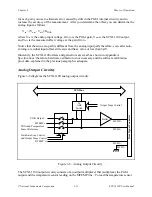
Figure 3-6 diagrams the SCXI-1100 analog input and timing circuitry.

Содержание 776572-00

Страница 1: ...ht 1991 1994 National Instruments Corporation All Rights Reserved SCXI 1100 User Manual 32 Channel Differential Multiplexer Amplifier Module for Signal Conditioning October 1994 Edition Part Number 32...

Страница 2: ...ria 0662 435986 Belgium 02 757 00 20 Canada Ontario 519 622 9310 Canada Qu bec 514 694 8521 Denmark 45 76 26 00 Finland 90 527 2321 France 1 48 14 24 24 Germany 089 741 31 30 Italy 02 48301892 Japan 0...

Страница 3: ...RIGHT TO RECOVER DAMAGES CAUSED BY FAULT OR NEGLIGENCE ON THE PART OF NATIONAL INSTRUMENTS SHALL BE LIMITED TO THE AMOUNT THERETOFORE PAID BY THE CUSTOMER NATIONAL INSTRUMENTS WILL NOT BE LIABLE FOR...

Страница 4: ...or application designer Any use or application of National Instruments products for or involving medical or clinical treatment must be performed by properly trained and qualified medical personnel an...

Страница 5: ...tion 2 5 Grounding Shielding and Output Mode Selection 2 6 Jumper W10 2 6 Reference Mode Selection 2 7 Jumper W1 2 7 Filter Selection 2 7 Jumpers W2 through W4 2 7 Output Selection 2 8 Jumpers W7 and...

Страница 6: ...ing Indirect 3 15 Multiple Module Multiplexed Scanning 3 15 Multiple Chassis Scanning 3 16 Chapter 4 Register Descriptions 4 1 Register Description 4 1 Register Description Format 4 1 SCXI 1100 Regist...

Страница 7: ...t A 3 Appendix B Rear Signal Connector B 1 Rear Signal Connector Signal Descriptions B 2 Appendix C SCXIbus Connector C 1 SCXIbus Connector Signal Descriptions C 3 Appendix D SCXI 1100 Front Connector...

Страница 8: ...CXI 1350 Multichassis Adapter E 12 SCXI 1350 Installation E 13 SCXI 1343 Rear Screw Terminal Adapter E 13 SCXI 1343 Installation E 13 Appendix F Revision A and B Photo and Parts Locator Diagram F 1 Ap...

Страница 9: ...Block Diagram 3 2 Figure 3 3 SCXIbus Connector Pin Assignment 3 4 Figure 3 4 Digital Interface Circuitry Block Diagram 3 7 Figure 3 5 SCXI 1100 Digital Control Circuitry 3 8 Figure 3 6 Analog Input an...

Страница 10: ...rent Receiver Resistors 2 10 Table 2 8 Jumper Setting on the Terminal Block 2 20 Table 2 9 SCXIbus to SCXI 1100 Rear Signal Connector to Data Acquisition Board Pin Equivalences 2 25 Table 3 1 SCXIbus...

Страница 11: ...ns how to unpack the SCXI 1100 kit Chapter 2 Configuration and Installation describes the SCXI 1100 jumper configurations installation of the SCXI 1100 into the SCXI chassis signal connections to the...

Страница 12: ...mputers MIO board MIO board refers to the AT MIO 16 AT MIO 16D AT MIO 16F 5 AT MIO 16X AT MIO 64F 5 MC MIO 16 NB MIO 16 and NB MIO 16X multichannel I O data acquisition boards unless otherwise noted m...

Страница 13: ...PC User Manual part number 320502 01 MC MIO 16 User Manual Revisions A to C part number 320130 01 MC MIO 16 User Manual Revision D part number 320560 01 NB MIO 16 User Manual part number 320295 01 NB...

Страница 14: ...0 with other systems that comply with the specifications given in Chapter 2 Configuration and Installation Each SCXI 1100 module multiplexes its 32 input channels into a single channel of the data acq...

Страница 15: ...data acquisition boards NI DAQ has a library of functions that you can call from your application programming environment These functions include routines for analog input A D conversion buffered data...

Страница 16: ...adapter 776574 46 SCXI 1347 SCXI shielded cable assembly with 1 m cable with 2 m cable with 5 m cable with 10 m cable 776574 471 776574 472 776574 475 776574 470 SCXI 1349 SCXI shielded cable assembl...

Страница 17: ...pin DIN C male connector The manufacturer part number of this connector National Instruments uses is as follows Harting Electronik Inc part number 09 03 396 6921 The mating connector for the SCXI 110...

Страница 18: ...ons installation of the SCXI 1100 into the SCXI chassis signal connections to the SCXI 1100 and cable wiring Module Configuration Revision C and later SCXI 1100 modules contain 10 jumpers that are sho...

Страница 19: ......

Страница 20: ...C coupled sources Jumpers W2 through W4 are used to set the lowpass filter LPF or full bandwidth FBW Further configuration of the board is software controlled and is discussed later in this chapter Di...

Страница 21: ...efault position position 1 On all but one of the SCXI 1100s that are cabled to the data acquisition board move jumper W9 to position 3 It does not matter which of the SCXI 1100 modules that are cabled...

Страница 22: ...hich is reserved Table 2 1 Digital Signal Connections Jumper Settings Jumper Description Configuration W5 Connects MISO to SERDATOUT factory default setting 1 2 3 W5 Parking position 1 2 3 W6 Factory...

Страница 23: ...ve a nonreferenced single ended input NRSE Do not use differential input data acquisition boards when jumper W10 is in the AB R2 position Table 2 2 Jumper W10 Settings Jumper Description Configuration...

Страница 24: ...00 k resistor to the negative input of the amplifier to prevent saturation of the amplifier inputs This reduces the input impedance however and usually increases settling time and common mode noise Al...

Страница 25: ...ing time varies greatly when you configure the SCXI 1100 to a 4 Hz or 10 kHz filter or full bandwidth Refer to Appendix A Specifications for details on how fast you can scan in each case Output Select...

Страница 26: ...onds to which input channel Table 2 6 User Defined Input Filter Capacitors Input Channel Spare Capacitor Reference Designator 0 C1 1 C5 2 C4 3 C2 4 through 7 C10 through C7 respectively 8 through 11 C...

Страница 27: ...Take off the rear panel by removing the two other screws 3 Slide the module out of its enclosure 4 Insert the capacitor s and or resistor s into their appropriate pads 5 Solder the leads to the pads o...

Страница 28: ...connect additional cabling to the SCXI 1100 Typically only one module in a chassis is cabled to a data acquisition board For installation procedures with other SCXI accessories and data acquisition bo...

Страница 29: ...6 5 4 3 2 1 5 V CGND MTEMP DTEMP CGND GUARD AOREF OUTPUT CGND CGND CGND CH0 CH0 CH1 CH1 CH2 CH2 CH3 CH3 CH4 CH4 CH5 CH5 CH6 CH6 CH7 CH7 CH8 CH8 CH9 CH9 CH10 CH10 CH11 CH1 CH12 CH12 CH13 CH13 CH14 CH1...

Страница 30: ...ed in the Analog Configuration section B1 B32 CH31 through CH0 Negative Input Channels Negative input channels to the PGIA C1 C32 CH31 through CH0 Positive Input Channels Positive input channels to th...

Страница 31: ...Chapter 2 SCXI 1100 User Manual 2 14 National Instruments Corporation 100 k Vout Vcm VS PGIA W1 Position 1 2 Figure 2 3 Ground Referenced Signal Connection 100 k Vout VS PGIA W1 Position 2 3 Figure 2...

Страница 32: ...equation Vofsbias Iofsbias Rbias Rbias 100 k Ibias Use a 100 k value when you use jumper W1 to reduce the amount of offset as well as to maintain a balanced input and avoid the degradation of the PGIA...

Страница 33: ...minals can damage the SCXI 1100 the SCXIbus backplane and the data acquisition board National Instruments is not liable for any damages resulting from such signal connections Thermocouple Connections...

Страница 34: ...jumpers as described in the Output Selection section earlier in this chapter When you do not need the module output at the front connector place jumpers W7 and W8 in position B thus connecting pins A8...

Страница 35: ...ack screw 9 Repeat steps 6 through 8 for the second jack screw 10 Replace the module cover and tighten the grounding screw 11 Slide the module back into place in the chassis 12 Connect the connector a...

Страница 36: ...data acquisition channel via MCH1 pins 5 and 6 on the rear signal connector The temperature sensor outputs 10 mV C and has an accuracy of 0 9 C over the 0 to 55 C temperature range To determine the te...

Страница 37: ...e Phillips head number 2 screwdriver slide the signal wires one at a time through the front panel strain relief opening Add insulation or padding if necessary 4 Connect the wires to the screw terminal...

Страница 38: ......

Страница 39: ...through panel the SCXI 1343 rear screw terminal adapter or the SCXI 1351 one slot cable extender with the SCXI 1100 you should read this section Figure 2 8 shows the pin assignments for the SCXI 1100...

Страница 40: ...erial Data Out Taps into the SCXIbus MISO line to accept serial output data from a module 27 DAQD A Data Acquisition Board Data Address Line Taps into the SCXIbus D A line to indicate to the module wh...

Страница 41: ...arlier in this chapter Warning The SCXI 1100 analog outputs are not overvoltage protected Applying external voltage to these outputs can damage the SCXI 1100 National Instruments is not liable for any...

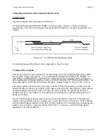
Страница 42: ...1 PB5 DOUT5 INTR SLOT0SEL ADIO2 PB6 DOUT6 SPICLK SERCLK EXTSTROBE PB7 DOUT7 MISO SERDATOUT BDIO0 PC1 DIN6 The digital timing signals are pins 36 and 43 Pin 36 is a SCXI 1100 clock that increments the...

Страница 43: ...RCLK Furthermore Slot 0 produces SS according to data acquisition board programming so this section also describes SS timing relationships For more information on the Slot 0 Slot Select Register consu...

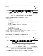
Страница 44: ...EL to 0 This deasserts all SS lines to all modules in all chassis 3 For each bit starting with the MSB perform the following actions a Set SERDATIN bit to be sent These bits are the data that is being...

Страница 45: ...r the 32 bits of data are read from the Module ID Register further data will be zeros until reinitialization occurs To write to the Configuration Register perform the following steps 1 Initial conditi...

Страница 46: ...bit to be read Clear SERCLK to 0 Set SERCLK to 1 Clock the data Read the level of the SERDATOUT line 3 Pull SLOT0SEL low to deassert the SS line and establish conditions for writing a new slot select...

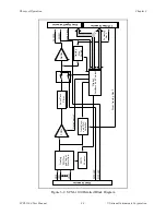
Страница 47: ...the operation of each functional unit making up the SCXI 1100 Functional Overview The block diagram in Figure 3 1 illustrates the key functional components of the SCXI 1100 Figure 3 2 shows the detail...

Страница 48: ...nter PGIA Analog MUXes and Input Protection Auto Zero and CAL Switches Low Pass Filter Gain Control CH0 CH1 CH31 From Analog Bus 2 Digital Interface and Control Analog Bus Switch To Analog Bus 0 SCXIb...

Страница 49: ...ur to one dual multiplexers for a total of 32 differential channels and a PGIA with gains of 1 2 5 10 20 50 100 200 500 1 000 and 2 000 The SCXI 1100 also has a digital section for automatic control o...

Страница 50: ...2 D3 C3 D4 C4 D5 C5 D6 C6 D7 C7 D8 C8 D9 C9 D10 C10 D11 C11 D12 C12 D13 C13 D14 C14 D15 C15 D16 C16 D17 C17 D18 C18 D19 C19 D20 C20 D21 C21 D22 C22 D23 C23 D24 C24 GUARD GUARD GUARD AB0 GUARD GUARD GU...

Страница 51: ...e analog bus 2 line Refer to the Calibration section later in this chapter for information on the use of this pin C13 C17 A21 CHSGND Chassis Ground Digital and analog ground B21 C21 D21 reference C18...

Страница 52: ...le high clock and second edge data latching D A INTR and RESET are additional control signals When the module is installed in an SCXI 1000 or SCXI 1001 chassis the data acquisition board via the modul...

Страница 53: ...hows a diagram of the SCXI 1100 and SCXIbus digital interface circuitry Digital Interface SCXIbus Buffered Serial Data Buffered Digital Control Signals SERDATIN DAQD A SLOT0SEL SERCLK SERDATOUT Rear S...

Страница 54: ...cquisition board when SS is enabled and D A indicates data transfer D A low You use the Configuration Register for channel gain calibration and auto zeroing selection in addition to configuring the SC...

Страница 55: ...18 5 VDC that is regulated on the SCXI 1100 to 15 VDC a guard analog buses AB0 AB2 and a chassis ground CHSGND AB0 buses the SCXI 1100 output to other modules or receives outputs from other modules v...

Страница 56: ...Hardware PGIA Input Channel Select Calibration or Input Selection Auto Zero or Auto Calibration Selection From AB2 Gain Select Timing Signals To Output Multiplexer Figure 3 6 Analog Input and Timing B...

Страница 57: ...put signal into a single ended signal with respect to the SCXI 1100 ground for input common mode signal rejection With this conversion the module can extract the input analog signal from a common mode...

Страница 58: ...and Current Loop Resistors section in Chapter 2 Configuration and Installation for more information Calibration The calibration hardware consists of two single pole double throw SPDT switches After y...

Страница 59: ...put offset still exists and has a value of less than 5 V Inherently the SCXI 1100 offsets and gain errors are small as shown in Appendix A Specifications therefore hardware calibration is not necessar...

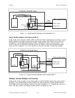
Страница 60: ...o simulate scanning In these cases the Lab boards or the PC LPM 16 board may be sufficient For additional information consult either Chapter 2 Configuration and Installation Chapter 5 Programming your...

Страница 61: ...ta acquisition board The SCXI 1100 receives its MUXCOUNTER clock from TRIG0 which the intermediate module sends as shown in Figure 3 10 Slot 0 operation is the same for direct connection scanning Cabl...

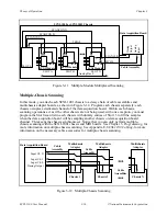
Страница 62: ...erations act as if the other chassis are not being used with one exception you must program the Slot 0 scan list in each chassis with dummy entries of Slot 13 to fill the samples when the data acquisi...

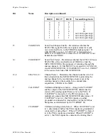
Страница 63: ...ch bit The register bit map shows a diagram of the register with the MSB shown on the left bit 15 for a 16 bit register bit 7 for an 8 bit register and the LSB shown on the right bit 0 A rectangle is...

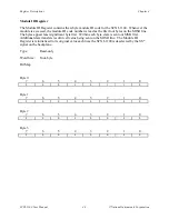
Страница 64: ...e bytes appear least significant byte first Within each byte data is sent out MSB first Additional data transfers result in all zeros being sent on the MISO line The Module ID Register is reinitialize...

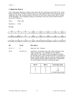
Страница 65: ...ap 23 22 21 20 19 18 17 16 X X X GAIN4 GAIN3 GAIN2 GAIN1 GAIN0 15 14 13 12 11 10 9 8 CLKOUTEN CLKSELECT X CHAN4 CHAN3 CHAN2 CHAN1 CHAN0 7 6 5 4 3 2 1 0 CAL ENM CV ZERO RTEMP RSVD SCANCLKEN SCANCONEN A...

Страница 66: ...UNTER If CLKSELECT is set to 1 TRIG0 is the source that clocks MUXCOUNTER 12 8 CHAN 4 0 Channel Select Determine the channel number 0 to 31 that is loaded into the MUXCOUNTER to determine the analog c...

Страница 67: ...CLKEN is set to 1 MUXCOUNTER will not be clocked 2 SCANCONEN Scan Control Enable When set to 1 enables the SCANCON signal 1 AB0EN Analog Bus 0 Enable Determines whether Analog Bus 0 on the SCXIbus dri...

Страница 68: ...ister is written to over the SLOT0SEL line Write to the HSCR and the FIFO Register as if they were registers on modules in Slots 13 and 14 Maintain software copies of the Slot Select Register HSCRs an...

Страница 69: ...ss of the chassis number written The Slot Select Register shifts in the data present on the MOSI line bit 16 first when SLOT0SEL is low Type Write only Word Size 16 bit Bit Map 15 14 13 12 11 10 9 8 X...

Страница 70: ...t is set to 1 it has no effect 5 RD Read When cleared to 0 prevents the FIFO from being read When set to 1 the FIFO is read except at the end of a scan list entry during scanning when reading is brief...

Страница 71: ...secutive writes to the FIFO Register create the Slot 0 scan list Each write creates a new entry at the end of the scan list The maximum number of entries is 256 To clear the FIFO of all entries clear...

Страница 72: ...be loaded into the MUXCOUNTER This value is either the channel to be read for single reads or a starting channel for scanned measurements The 24 bit patterns are presented MSB first left to right Reg...

Страница 73: ...an MIO board writing to the EXTSTROBE register will pulse EXTSTROBE low and then high accomplishing steps 3b and 3c 4 Set SLOT0SEL to 1 This asserts the SS line of the module whose slot number was wri...

Страница 74: ...subsequent channels The module is disconnected from Analog Bus 0 The total amplifier gain is 1 Single Channel Measurements This section describes how to program the SCXI 1100 either alone or in conjun...

Страница 75: ...XXX 00101011 to the SCXI 1100 Configuration Register This step disables the SCXI 1100 from driving Analog Bus 0 and allows Analog Bus 0 to drive MCH0 through the output buffer 3 Program the other modu...

Страница 76: ...AB0EN and or set FOUTEN in the Configuration Register 2 Program the other module not to drive Analog Bus 0 but to send Analog Bus 0 to the data acquisition board 3 Write the binary pattern XXXGGGGG 0...

Страница 77: ...Pseudo Simultaneous AT MIO 16F 5 User Manual Posttrigger Data Acquisition with Continuous Channel Scanning Posttrigger Data Acquisition with Interval Channel Scanning AT MIO 16X User Manual Continuous...

Страница 78: ...XI 1100s in one chassis to one MIO board channel often the simplest way to program the MIO board is to use only one data acquisition board scan list entry and make N the total number of samples to be...

Страница 79: ...0000101 to the SCXI 1100 Configuration Register CCCCC represents the starting channel number Single Module Multiplexed Scanning Indirect Channel Scanning from Other Modules To scan measurements from o...

Страница 80: ...0 to the data acquisition board but not drive Analog Bus 0 unless it is receiving an active low signal on SCANCON Also program the other module to send a SCANCLK compatible signal onto TRIG0 If this m...

Страница 81: ...ult the SCXI 1000 1001 User Manual Descriptions of the Slot 0 registers are given in the Slot 0 Register Descriptions section in Chapter 4 Register Descriptions To program the hardscan circuitry perfo...

Страница 82: ...ervicing At this point you should now continue from where you left off in the 1 Data Acquisition Board Setup Programming section of this chapter Perform the following steps given in your data acquisit...

Страница 83: ...module including the clearing of the AB0EN bit bit 0 Notice that a complete reset of this module is not necessary but is used for simplicity 3 Performing the procedure given in the Register Writes sec...

Страница 84: ...t Entry Slot Number Count 1 4 31 1 13 31 1 13 38 2 13 35 2 11 7 2 3 3 3 13 28 3 8 25 Other solutions are possible Perform the steps outlined in the 3 Programming the Slot 0 Hardscan Circuitry section...

Страница 85: ...Programming Chapter 5 SCXI 1100 User Manual 5 14 National Instruments Corporation 15 Toggle SLOT0SEL 16 Write XXXXX011 10011001 over MOSI 17 Select Slot 0 in Chassis 0...

Страница 86: ...0 pA Gain software selectable 1 2 5 10 20 50 100 200 500 1 000 2 000 Input impedance 1 G Settling time with 10 V step Full bandwidth Accuracy Gain 1 100 200 500 1 000 2 000 0 012 2 6 s 7 s maximum 7 5...

Страница 87: ...o 5 78 dB minimum Gain 10 to 2 000 90 dB minimum 4 Hz bandwidth Gain 1 to 5 98 dB minimum Gain 10 to 2 000 110 dB minimum Offset voltage Output uncalibrated 1 mV typical 3 mV maximum Output calibrated...

Страница 88: ...l Dimensions 1 2 by 6 8 by 8 0 in Connectors 50 pin male ribbon cable rear connector 96 pin DIN C front connector 70 screw terminal adapter available Cold Junction Sensor4 Accuracy 0 9 C over 0 to 55...

Страница 89: ...ption of each connection Figure B 1 shows the pin assignments for the SCXI 1100 rear signal connector 1 2 3 4 5 6 7 8 9 10 11 12 13 14 15 16 17 18 19 20 21 22 23 24 25 26 27 28 29 30 31 32 33 34 35 36...

Страница 90: ...rial input data to a module or Slot 0 26 SERDATOUT Serial Data Out Taps into the SCXIbus MISO line to accept serial output data from a module 27 DAQD A Data Acquisition Board Data Address Line Taps in...

Страница 91: ...1100 User Manual Appendix C SCXIbus Connector This appendix describes the pinout and signal names for the SCXI 1100 96 pin SCXIbus connector including a description of each connection Figure C 1 shows...

Страница 92: ...2 D3 C3 D4 C4 D5 C5 D6 C6 D7 C7 D8 C8 D9 C9 D10 C10 D11 C11 D12 C12 D13 C13 D14 C14 D15 C15 D16 C16 D17 C17 D18 C18 D19 C19 D20 C20 D21 C21 D22 C22 D23 C23 D24 C24 GUARD GUARD GUARD AB0 GUARD GUARD GU...

Страница 93: ...e analog bus 2 line Refer to the Calibration section later in this chapter for information on the use of this pin C13 C17 A21 CHSGND Chassis Ground Digital and analog ground B21 C21 D21 reference C18...

Страница 94: ...he module Open collector I O A24 TRIG0 TRIG0 General purpose trigger line that the SCXI 1100 uses to send SCANCLK to other modules or receive SCANCLK from other modules Open collector I O B24 SS Slot...

Страница 95: ...olumn A B C Signal Name 32 31 30 29 28 27 26 25 24 23 22 21 20 19 18 17 16 15 14 13 12 11 10 9 8 7 6 5 4 3 2 1 5 V CGND MTEMP DTEMP CGND GUARD AOREF OUTPUT CGND CGND CGND CH0 CH0 CH1 CH1 CH2 CH2 CH3 C...

Страница 96: ...irect Temperature Sensor Connects the temperature sensor to the MCH1 signal when the terminal block is configured for direct temperature connection A6 GUARD Guard Connected to the SCXIbus guard A7 AOR...

Страница 97: ...attaches to the MIO board I O connector Attached to the mounting bracket is a 50 pin female mounting bracket connector that connects to the module rear signal connector A male breakout connector is n...

Страница 98: ...H1 ACH1 6 MCH1 ACH9 19 OUTREF AISENSE 24 33 DIG GND DIG GND 25 SERDATIN ADIO0 26 SERDATOUT BDIO0 27 DAQD A ADIO1 29 SLOT0SEL ADIO2 36 SCANCLK SCANCLK 37 SERCLK EXTSTROBE 43 RSVD OUT1 No other pins are...

Страница 99: ...cable assembly connects a Lab LC board to an SCXI 1100 module The SCXI 1341 and SCXI 1344 cable assemblies consist of two pieces an adapter board and a 50 conductor ribbon cable that connects the Lab...

Страница 100: ...signal connector SCXI 1341 and SCXI 1344 Installation Perform the following steps to install the SCXI 1341 and SCXI 1344 1 Make sure that the computer and the SCXI chassis are turned off 2 Install th...

Страница 101: ...gital control lines but the PC LPM 16 can take only single measurements and cannot scan channels Leave jumper W1 in position A on the SCXI 1342 The SCXI 1100 does not use jumper W1 Table E 3 lists the...

Страница 102: ...connect to the SCXI 1100 This connector has an MIO 16 compatible pinout the pin equivalences of the MIO board on this connector and the SCXI 1100 are given in Table E 1 in the SCXI 1340 Cable Assembly...

Страница 103: ...se steps is not critical however it is easier to locate the correct position for the mounting bracket with a module installed in the chassis If you are attaching a cable to the female connector instal...

Страница 104: ...t panel connector has the feedthrough connection You can attach an SCXI 1302 terminal block to the front panel connector for simple screw terminal connections A rear filler panel that shields and prot...

Страница 105: ...Figure E 3 SCXI 1180 Rear Connections 4 Screw in the rear panel to the threaded strip in the rear of the chassis 5 Screw the front panel into the front threaded strip as shown in Figure E 4 Check the...

Страница 106: ...block has screw terminal connections for the 50 pin connector on the SCXI 1180 feedthrough panel SCXI 1302 Wiring Procedure To wire the SCXI 1302 terminal block you must remove the cover connect all t...

Страница 107: ...to Pry Open Figure E 5 Cover Removal SCXI 1302 Installation Perform the following steps to install the SCXI 1302 1 Install an SCXI 1180 feedthrough panel as described in the SCXI 1180 Installation se...

Страница 108: ...to the module rear signal connector Make sure the alignment tab on the bracket enters the upper board guide of the chassis 5 Screw the mounting bracket to the threaded strips in the rear of the chass...

Страница 109: ...two chassis connect the loose end of the ribbon cable to the rear connector of the second SCXI 1350 and install the adapter board 9 Continue until all chassis are connected For N chassis you will nee...

Страница 110: ...nal 17 No Connect Screw terminal 18 No Connect Screw terminal 19 OUTREF Screw terminal 20 No Connect Solder pad 21 No Connect Solder pad 22 No Connect Solder pad 23 No Connect Solder pad 24 33 DIG GND...

Страница 111: ...Photo and Parts Locator Diagram This appendix contains a photograph of the Revision A and B SCXI 1100 and the parts locator diagram Figure F 1 shows the Revision A and B SCXI 1100 Figure F 2 shows the...

Страница 112: ......

Страница 113: ...ay from 8 00 a m to 6 00 p m central time In other countries contact the nearest branch office You may fax questions to us at any time Corporate Headquarters 512 795 8248 Technical support fax 800 328...

Страница 114: ...ficiently If you are using any National Instruments hardware or software products related to this problem include the configuration forms from their user manuals Include additional pages if necessary...

Страница 115: ...arked W1 1 2 Filter Selection _________________________________________________ Factory Setting no filter W2 Grounding Shielding and Output Selection _________________________________________________...

Страница 116: ...Edition Date October 1994 Part Number 320637C 01 Please comment on the completeness clarity and organization of the manual If you find errors in the manual please record the page numbers and describe...

Страница 117: ...receiver resistors 2 10 user defined input filter capacitors 2 9 analog input and timing circuits 3 9 to 3 12 analog input channels AC coupled signal connection 2 15 exceeding input ranges warning 2...

Страница 118: ...4 4 CLKSELECT bit 4 4 CNT 3 0 bit 4 9 cold junction reference CJR included on SCXI 1100 1 1 specifications A 3 common mode rejection ratio specifications A 2 communication signals communicating on Se...

Страница 119: ...mory chip 3 14 FIFO Register description of 4 9 writing to registers 5 1 filtering specifications A 2 FOUTEN bit 4 5 front connector AC coupled connection 2 15 analog input channels 2 13 to 2 16 analo...

Страница 120: ...CH1 signal analog output 2 17 2 24 analog output circuitry 3 13 to 3 14 description of 2 23 B 2 measurements See scanning measurements single channel measurements MISO signal buffering to SERDATOUT pi...

Страница 121: ...equivalents for rear signal connector 3 6 OUTPUT signal connecting to terminal block 2 19 description of 2 13 D 2 OUTREF signal analog output 2 24 description of 2 23 B 2 P physical specifications A 3...

Страница 122: ...signal 3 5 C 3 Reset button 5 3 resistors installing 2 10 user defined current receiver resistors 2 10 RSVD bit 4 5 4 8 RSVD signal 2 23 3 5 B 2 C 3 RTEMP bit 4 5 S SCANCLK signal analog input and tim...

Страница 123: ...lection and write procedure 5 2 to 5 3 SCXIbus equivalent 3 6 selecting slots 2 26 to 2 29 timing requirements 2 28 SERDATIN signal description of 2 23 B 2 register selection and write procedure 5 2 t...

Страница 124: ...of A 2 to A 3 cold junction reference A 3 common mode rejection ratio A 2 cross talk A 2 digital I O signal connections 2 25 filtering A 2 gain error at DC A 2 input protection A 2 instrumentation amp...

Страница 125: ...egative Analog Bus Number signal AB0EN Analog Bus 0 Enable bit ACH data acquisition board analog input channel number A D analog to digital ADC A D converter AOGND Analog Output Ground signal AOREF An...

Страница 126: ...Address Line signal D A digital to analog D A Data Address signal dB decibels DC direct current DIG GND Digital Ground signal DTEMP Direct Temperature Sensor signal DTS direct temperature sensor F F f...

Страница 127: ...MCH Negative Analog Output Channel Number signal MISO Master In Slave Out signal MOD Module Number bit MOSI Master Out Slave In signal MPW Microsoft Programmer s Workshop MSB most significant bit MTE...

Страница 128: ...SCXI Signal Conditioning eXtensions for Instrumentation bus SDK Software Developer s Kit sec seconds SERCLK Serial Clock signal SERDATIN Serial Data In signal SERDATOUT Serial Data Out signal SLOT Slo...

Отзывы: