NAT-AMC-ZYNQUP-FMC
T
ECHNICAL
R
EFERENCE
M
ANUAL
V1.1
F
UNCTIONAL
D
ESCRIPTION
- 12 -
4.
F
UNCTIONAL
D
ESCRIPTION
The
NAT-AMC-ZYNQUP-FMC
can be divided into a number of functional blocks, which are
described in the following paragraphs.
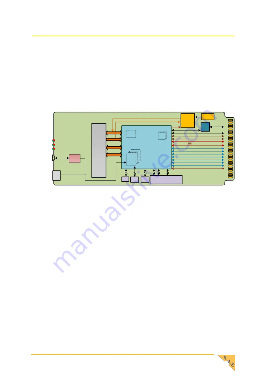
The following figure gives an overview on the functional blocks.
Figure 1
–
Block Diagram
JTAG
IPMI
MMC
I²C
GPU
SD
Card
JTAG to
USB +
UART
USB
FM
C
Co
nn
ec
to
r
V
IT
A
57
.1
-
H
P
C
AMC Ports 0/1 GbE
AMC Ports 2/3, 12-20 Custom
AMC Ports 4-11
PCIe / Ethernet / Custom
FPGA SerDes
FPGA SerDes
FPGA SerDes
FPGA SerDes
FPGA SerDes
FPGA SerDes
FPGA SerDes
FPGA SerDes
FPGA SerDes
FPGA SerDes
FPGA SerDes
TCLKA-D
FPGA
XILINX
Zynq MPSoC
Ult
FFVF1517
ZU7EG
ZU11EG
4x A53
ARM CPU
(Zynq)
2x
R5
2x
R5
CPU
Memory Extension Card:
2x 1GB DDR4 (x8) or
1x 144Mb QDR-IV SRAM (x18)
QSPI
FLASH
4
64
4GB
DDR4
64
4GB
DDR4
8
8
18
HPC IO
CLK_M2C
DP0-DP9
CLK2_BIDIR_C2M
GC
CLK0_M2C
Stratum III
CLK_BIDIR
Si5374
Clocking
4.1.
SoC
The central component on the
NAT-AMC-ZYNQUP-FMC
is
a Xilinx Zynq MPSoC Ult
FPGA device (ZYNQUP). This SoC provides a powerful general-purpose ARM-CPU, field-
programmable hardware accelerators (FPGA, DSP, and GPU), and flexible I/O.
GTH transceiver speed is 12.5 GHz per default assembly, other speed grades on request.
4.1.1.
Processing System (CPU)
The CPU core of the SoC features a quad-core ARM Cortex-A53 processor as application
processing unit and a dual-core ARM Cortex-R5 for real-time processing. Moreover, it is
equipped with a dedicated GPU, realized by a Mali-400 MP2 graphics processing unit.
4.1.1.1.
Memory
The Processing System is accompanied by up to 4GB DDR4 RAM (x64, 1600-2400Mb/s). On
board NAND and NOR flashes can be used for booting and configuring the SoC. The additional
MicroSD-Card slot at the front panel can also be used for that purpose but offers quicker
physical access, which is useful during the development.


