


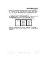
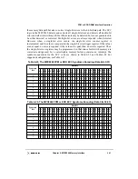

Chapter 6. MPC8240 Memory Interface
6-61
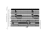
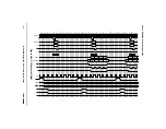
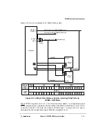
FPM or EDO DRAM Interface Operation
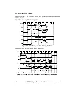
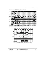
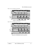
6.3.6 DMA Burst Wrap
The MPC8240 supports burst-of-four data beats for accesses with a 64-bit data path and
burst-of-eight data beats for accesses with a 32-bit data path. The burst is always sequential,
and the critical double word is always supplied first as detailed in the following two
examples:
•
Using a 64-bit data path, if the processor core requests the third double word (DW2)
of a cache line, the MPC8240 reads double words from memory in the order
DW2-DW3-DW0-DW1.
•
Using a 32-bit data path, if the processor core requests the third double word (W4
and W5) of a cache line, the MPC8240 reads words from memory in the order
W4-W5-W6-W7-W0-W1-W2-W3.
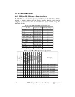
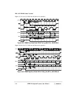
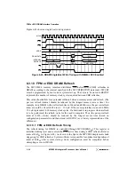
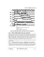
6.3.7 FPM or EDO DRAM Page Mode Retention
Under certain conditions, the MPC8240 retains the currently active FPM or EDO page by
holding RAS asserted for pipelined burst accesses. These conditions are as follows:
•
A pending transaction (read or write) hits the currently active FPM or EDO page.
•
There are no pending refreshes.
•
The maximum RAS assertion interval (controlled by PGMAX) has not been
exceeded.
Page mode can dramatically reduce access latencies for page hits. Depending on the
memory system design and timing parameters, page mode can save three to four clock
cycles from subsequent burst accesses that hit in an active page. Page mode is disabled by
clearing the PGMAX parameter (PGMAX = 0x00) located in the memory page mode
register (MPM). See Section 4.6.3, “Memory Page Mode Register—0xA3,” for more
information.
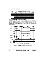
6.3.8 FPM or EDO DRAM Parity and RMW Parity
When configured for FPM or EDO, the MPC8240 supports two forms of parity checking
and generation—normal parity and read-modify-write (RMW) parity. Normal parity
assumes that each of the eight parity bits is controlled by a separate CAS signal. Thus, for
a single-beat write from PCI to system memory, the MPC8240 generates a parity bit for
each byte written to memory.
RMW parity assumes that all eight parity bits are controlled by a single CAS signal;
therefore it must be written as a single 8-bit quantity (byte). Thus, for any write operation
to system memory that is less than a double word, the MPC8240 must latch the write data,
read an entire 64-bit double word from memory, check the parity of that double word,
merge the write data with that double word, regenerate parity for the new double word, and
finally write the new double word back to memory.
Содержание MPC8240
Страница 1: ...MPC8240UM D Rev 1 1 2001 MPC8240 Integrated Processor User s Manual ...
Страница 38: ...xviii MPC8240 Integrated Processor User s Manual TABLES Table Number Title Page Number ...
Страница 48: ...xlviii MPC8240 Integrated Processor User s Manual Acronyms and Abbreviations ...
Страница 312: ...6 94 MPC8240 Integrated Processor User s Manual ROM Flash Interface Operation ...
Страница 348: ...7 36 MPC8240 Integrated Processor User s Manual PCI Host and Agent Modes ...
Страница 372: ...8 24 MPC8240 Integrated Processor User s Manual DMA Register Descriptions ...
Страница 394: ...9 22 MPC8240 Integrated Processor User s Manual I2O Interface ...
Страница 412: ...10 18 MPC8240 Integrated Processor User s Manual Programming Guidelines ...
Страница 454: ...12 14 MPC8240 Integrated Processor User s Manual Internal Arbitration ...
Страница 466: ...13 12 MPC8240 Integrated Processor User s Manual Exception Latencies ...
Страница 516: ...16 14 Watchpoint Trigger Applications ...
Страница 538: ...B 16 MPC8240 Integrated Processor User s Manual Setting the Endian Mode of Operation ...
Страница 546: ...C 8 MPC8240 Integrated Processor User s Manual ...
Страница 640: ...INDEX Index 16 MPC8240 Integrated Processor User s Manual ...


