


6-56
MPC8240 Integrated Processor User’s Manual
FPM or EDO DRAM Interface Operation
After configuration of all these parameters is complete, the system software must set the
configuration bit MEMGO which enables the memory controller. The MPC8240 performs
one CAS before RAS (CBR) refresh cycle each time REFINT elapses. After eight
refreshes, the main memory array is available for read and write accesses.
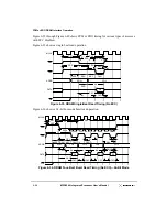
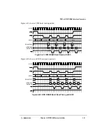
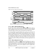
6.3.5 FPM or EDO DRAM Interface Timing
The read and write timing for DRAM is also controlled through programmable registers.
These registers are programmed by system software at system start-up to control:
•
RAS precharge time (RP
1
)
•
RAS to CAS delay time (RCD
2
)
•
CAS pulse width for the first access (CAS
3
)
•
CAS precharge time (CP
4
)
•
CAS pulse width in page mode (CAS
5
)
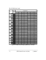
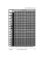
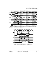
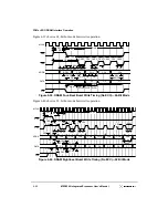
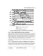
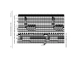
All signal transitions occur on system clock rising edges. Figure 6-36 shows DRAM read
timing with the programmable variables. Figure 6-38 shows DRAM write timing with the
programmable variables. As shown, the provided timing variables are applicable to both
read and write timing configuration. System software is responsible for optimal
configuration of these parameters after reset. This configuration process must be completed
at system start-up before any attempts to access DRAM. The actual values used by boot
code depend on the memory technology used.
Note that no more than 8 PCI clock cycles should elapse between successive assertions of
CAS within a burst.
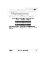
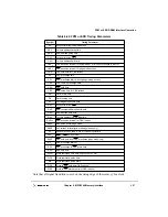
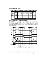
Table 6-22 defines the timing parameters for FPM or EDO DRAM. Subscripts identify
timing variables.
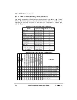
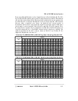
ECC_EN
ECC enable
MCCR2 @ <F4>
BUF_TYPE[1]
Registered data path = 0 (off)
MCCR4 @ <FC>
BUF_TYPE[0]
Cleared. In-line data path disabled.
MCCR4 @ <FC>
WRITE_PARITY_CHK
Enable write path parity error reporting
MCCR2 @ <F4>
Table 6-21. Memory Interface Configuration Register Fields (Continued)
Register Field
Description
Configuration
Register (and offset)
Содержание MPC8240
Страница 1: ...MPC8240UM D Rev 1 1 2001 MPC8240 Integrated Processor User s Manual ...
Страница 38: ...xviii MPC8240 Integrated Processor User s Manual TABLES Table Number Title Page Number ...
Страница 48: ...xlviii MPC8240 Integrated Processor User s Manual Acronyms and Abbreviations ...
Страница 312: ...6 94 MPC8240 Integrated Processor User s Manual ROM Flash Interface Operation ...
Страница 348: ...7 36 MPC8240 Integrated Processor User s Manual PCI Host and Agent Modes ...
Страница 372: ...8 24 MPC8240 Integrated Processor User s Manual DMA Register Descriptions ...
Страница 394: ...9 22 MPC8240 Integrated Processor User s Manual I2O Interface ...
Страница 412: ...10 18 MPC8240 Integrated Processor User s Manual Programming Guidelines ...
Страница 454: ...12 14 MPC8240 Integrated Processor User s Manual Internal Arbitration ...
Страница 466: ...13 12 MPC8240 Integrated Processor User s Manual Exception Latencies ...
Страница 516: ...16 14 Watchpoint Trigger Applications ...
Страница 538: ...B 16 MPC8240 Integrated Processor User s Manual Setting the Endian Mode of Operation ...
Страница 546: ...C 8 MPC8240 Integrated Processor User s Manual ...
Страница 640: ...INDEX Index 16 MPC8240 Integrated Processor User s Manual ...


