Chapter 6. MPC8240 Memory Interface
6-9
SDRAM Interface Operation
6.2.1 Supported SDRAM Organizations
It is not necessary to use identical memory chips in each memory bank; individual memory
banks may be of differing size. Although the MPC8240 multiplexes the row address,
column address, and logical bank select bits onto a shared 14-bit memory address bus,
individual SDRAM banks may be implemented with memory devices requiring fewer than
28 address bits. The MPC8240 can be configured to provide 12- or 11-row bits to a
particular bank, and 10, 9, 8, or 7 column bits, and 2 or 4 logical banks.
System software must configure the MPC8240 for the correct memory bank sizes. A
memory polling algorithm can be used at start-up to determine start and end of memory.
Alternately, many DIMMs have an on-board serial-presence-detect (SPD) EEPROM that
contains information about the size and timing requirements of the SDRAMs on the
DIMM. A software routine can use the I
2
C to read the SPD. Boot firmware can initially set
the SDRAM timing parameters with conservative values. Later, when the I
2
C routine reads
the SPD information from the DIMM, the timing parameters can be adjusted accordingly.
The MPC8240 uses its bank map to assert the appropriate CS[0:7] signal for memory
accesses according to the provided bank depths. System software must also configure the
MPC8240 at system start-up to appropriately multiplex the row and column address bits for
each bank. Refer to the row-address configuration in MCCR1. Address multiplexing occurs
according to these configuration bits.
If a disabled bank has its starting and ending address defined as overlapping an enabled
bank’s address space, there may be system memory corruption in the overlapping address
range. Any unused banks should have their starting and ending addresses programmed out
of the range of memory banks in use.
Table 6-4 shows the unsupported multiplexed row and column address bits for 32- and
64-bit modes. Configurations using 7 or 8 column address bits in 32-bit data bus mode and
7 column bits in 64-bit data bus mode are not supported as they would create
non-contiguous address spaces.
Table 6-5 summarizes the SDRAM memory configurations supported by the MPC8240.
Note that Table 6-5 is not an exhaustive list of all configurations that the MPC8240 can
support. The MPC8240 can support any device that can accept the address multiplexing
described in Section 6.2.2, “SDRAM Address Multiplexing,” without exceeding the 1
Gbyte limit on physical memory.
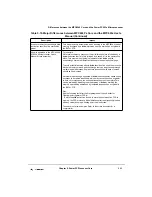
Table 6-4. Unsupported Multiplexed Row and Column Address Bits
32-bit Data Bus Mode
64-bit Data Bus Mode
13x8
—
12x8
—
11x8
—
12x7
12x7
Содержание MPC8240
Страница 1: ...MPC8240UM D Rev 1 1 2001 MPC8240 Integrated Processor User s Manual ...
Страница 38: ...xviii MPC8240 Integrated Processor User s Manual TABLES Table Number Title Page Number ...
Страница 48: ...xlviii MPC8240 Integrated Processor User s Manual Acronyms and Abbreviations ...
Страница 312: ...6 94 MPC8240 Integrated Processor User s Manual ROM Flash Interface Operation ...
Страница 348: ...7 36 MPC8240 Integrated Processor User s Manual PCI Host and Agent Modes ...
Страница 372: ...8 24 MPC8240 Integrated Processor User s Manual DMA Register Descriptions ...
Страница 394: ...9 22 MPC8240 Integrated Processor User s Manual I2O Interface ...
Страница 412: ...10 18 MPC8240 Integrated Processor User s Manual Programming Guidelines ...
Страница 454: ...12 14 MPC8240 Integrated Processor User s Manual Internal Arbitration ...
Страница 466: ...13 12 MPC8240 Integrated Processor User s Manual Exception Latencies ...
Страница 516: ...16 14 Watchpoint Trigger Applications ...
Страница 538: ...B 16 MPC8240 Integrated Processor User s Manual Setting the Endian Mode of Operation ...
Страница 546: ...C 8 MPC8240 Integrated Processor User s Manual ...
Страница 640: ...INDEX Index 16 MPC8240 Integrated Processor User s Manual ...

