
Chapter 2. Signal Descriptions and Clocking
2-33
Detailed Signal Descriptions
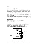
2.2.7.1 System Clock Input (OSC_IN)—Input
Provides the input to the PCI clock fanout buffer. A clock can be connected to this input to
provide multiple low-skew copies on the PCI_CLK[0:4] and PCI SYNC_OUT signals. For
systems that do not use the fanout buffer feature, this signal should be tied to a fixed state.
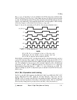
2.2.7.2 PCI Clock (PCI_CLK[0:4])—Output
These signals provide multiple copies of OSC_IN as output signals when using the PCI
clock fanout buffer feature. If these outputs are not needed, they can be individually
disabled in the CDCR register to minimize power consumption.
2.2.7.3 PCI Clock Synchronize Out (PCI_SYNC_OUT)—Output
This output is an additional clock provided by the PCI clock fanout buffer. It is intended to
be fed into the PCI_SYNC_IN signal to allow the internal clock subsystem to synchronize
to the system PCI clocks.
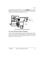
2.2.7.4 PCI Feedback Clock (PCI_SYNC_IN)—Input
This signal provides the input to the peripheral logic PLL. The PLL multiplies up and
synchronizes to this reference clock. The frequency of the PLL outputs is based on the PLL
clock frequency configuration signal settings at reset. See the MPC8240 Hardware
Specification for a complete listing of supported PLL_CFG[0:4] settings.
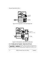
2.2.7.5 SDRAM Clock Outputs (SDRAM_CLK[0:3])—Output
The MPC8240 provides four low-skew copies of the SDRAM clock for use in small
memory subsystems. This clock is synchronized to the on-chip logic using a DLL. If these
outputs are not needed, they can be individually disabled in the CDCR register to minimize
power consumption.
2.2.7.6 SDRAM Clock Synchronize Out
(SDRAM_SYNC_OUT)—Output
SDRAM_SYNC_OUT is an advanced version of the SDRAM clock provided to allow
feedback into the DLL to allow proper compensation for the output and flight time delay of
the clock path.
2.2.7.7 SDRAM Feedback Clock (SDRAM_SYNC_IN)—Input
The SDRAM_SYNC_OUT signal should be connected to the SDRAM_SYNC_IN signal
to allow the on -chip DLL to synchronize and compensate for routing delays and the output
buffer.
For systems that use an external PLL to provide the clock source to SDRAM, this signal
can be pulled high unless the SDRAM clock-to-PCI clock ratio is non-integer (3:2 or 5:2).
In that case, this signal is used to synchronize between the internal clock and the external
SDRAM clock.
Содержание MPC8240
Страница 1: ...MPC8240UM D Rev 1 1 2001 MPC8240 Integrated Processor User s Manual ...
Страница 38: ...xviii MPC8240 Integrated Processor User s Manual TABLES Table Number Title Page Number ...
Страница 48: ...xlviii MPC8240 Integrated Processor User s Manual Acronyms and Abbreviations ...
Страница 312: ...6 94 MPC8240 Integrated Processor User s Manual ROM Flash Interface Operation ...
Страница 348: ...7 36 MPC8240 Integrated Processor User s Manual PCI Host and Agent Modes ...
Страница 372: ...8 24 MPC8240 Integrated Processor User s Manual DMA Register Descriptions ...
Страница 394: ...9 22 MPC8240 Integrated Processor User s Manual I2O Interface ...
Страница 412: ...10 18 MPC8240 Integrated Processor User s Manual Programming Guidelines ...
Страница 454: ...12 14 MPC8240 Integrated Processor User s Manual Internal Arbitration ...
Страница 466: ...13 12 MPC8240 Integrated Processor User s Manual Exception Latencies ...
Страница 516: ...16 14 Watchpoint Trigger Applications ...
Страница 538: ...B 16 MPC8240 Integrated Processor User s Manual Setting the Endian Mode of Operation ...
Страница 546: ...C 8 MPC8240 Integrated Processor User s Manual ...
Страница 640: ...INDEX Index 16 MPC8240 Integrated Processor User s Manual ...


