7-10
Error Messages
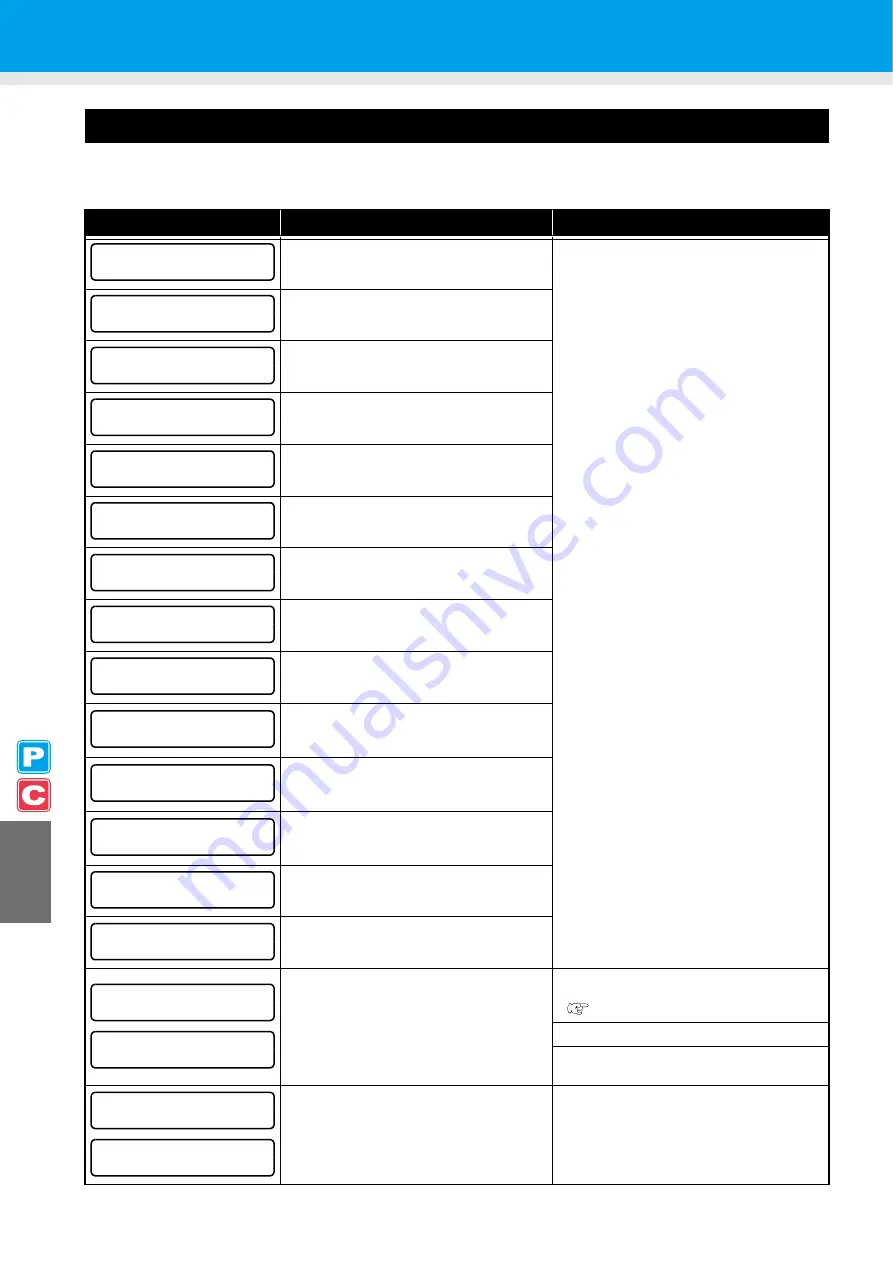
When an error message is displayed, eliminate the error according to the chart below.
If the same error message appears again, contact your distributor or our service office.
Error messages
Cause
Solution
An error occurred in the circuit board system.
(ROM)
Turn OFF the power to the machine and turn it
ON again after a while.
If the same error message appears again,
contact our service office or the distributor in your
region.
An error occurred in the circuit board system.
(RAM)
An error occurred in the circuit board system.
(Power supply v5 V)
An error occurred in the circuit board system.
(Power supply v24 V)
An error occurred in the circuit board system.
(Power supply v42 V)
An error occurred in the circuit board system.
(Parameter ROM)
An error occurred in the circuit board system.
(SDRAM)
A connection error in the heads was detected.
(Abnormal temperature was detected.)
A connection error in the heads was detected.
(Abnormal voltage was detected.)
An error occurred in detecting the linear
encoder.
(Unable to count)
An error occurred in detecting the linear
encoder.
(Error in the mounting direction)
An error occurred in detecting the linear
encoder.
(Read-out count error)
An error occurred in the circuit board system.
(FPGA PDC)
An error occurred in the circuit board system.
(FPGA HDC)
The machine received some data other than
command data.
According to the application, switch the settings
for COMMON SETUP>RECEIVED DATA.
(
Securely connect the interface cable in position.
Use an interface cable conforming to the
specifications.
Any parameter outside the range of acceptable
numeric values was received.
Turn OFF the power to the machine and turn it
ON again after a while.
If the same error message appears again,
contact our service office or the distributor in your
region.
* * * * * E R R OR 0 1
* * * * *
M A I N R OM
* * * * * E R R OR 0 2
* * * * *
M A I N R A M
* * * * * E R R OR 0 3
* * * * *
P OWE R + 5 V
* * * * * E R R OR 0 3
* * * * *
P OWE R + 2 4 V
* * * * * E R R OR 0 3
* * * * *
P OWE R + 4 2 V
* * * * * E R R OR 0 4
* * * * *
F - R OM
* * * * * E R R OR 0 6
* * * * *
S D - R A M
* * * * * E R R OR 0 7
* * * * *
H E A D ( - - - - )
* * * * * E R R OR 0 7
* * * * *
V O L T A G E
( - - - - )
* * * * * E R R OR 0 8
* * * * *
L i n e a r E N C OD E R : S E N S OR
* * * * * E R R OR 0 8
* * * * *
L i n e a r E N C OD E R : D I R .
* * * * * E R R OR 0 8
* * * * *
L i n e a r E N C OD E R : C O U N T
* * * * * E R R OR 0 9
* * * * *
F P G A E R R OR
* * * * * E R R OR 0 9
* * * * *
H D C E R R OR ( - - - - )
* * * * * E R R OR 1 0
* * * * *
C OMM A N D E R R O R
* * * * E R R OR 1 0 - C * * * *
C OMM A N D E R R O R
* * * * * E R R OR 1 1
* * * * *
P A R A M E T E R E R R O R
* * * * E R R OR 1 1 - C * * * *
P A R A M E T E R E R R O R
Содержание CJV30-100
Страница 15: ...xiv How to Read this Manual...
Страница 16: ...xv...
Страница 158: ...Other Convenient Functions 4 48 12 Press the key...
Страница 239: ...Warning Labels 8 7 8 Appendix No Order No Label 1 M904810 2 M905935 3 M905811 4 M903330 5 M903239 6 M903405...
Страница 243: ...8 11 Function Flowchart 8 Appendix MED I A RES I DUA L PR I NT ENT Only when MEDIA RESIDUAL is ON...
Страница 244: ...8 12 ES 3 I NK MMCCYYKK REMA I N 3 4 5 6 7 8 9 9 HEAD HE I GHT T h i n MMMMMMM 1 0 0 0mm From P8 10...
Страница 261: ...8 29 Function Flowchart 8 Appendix...
Страница 269: ...8 37 Function Flowchart 8 Appendix...
Страница 272: ...8 40...
Страница 273: ...D201873 11 26092008...
Страница 274: ...NH FW 1 1 MIMAKI ENGINEERING CO LTD 2008...


