Introduction
UG0557 User Guide Revision 4.0
4
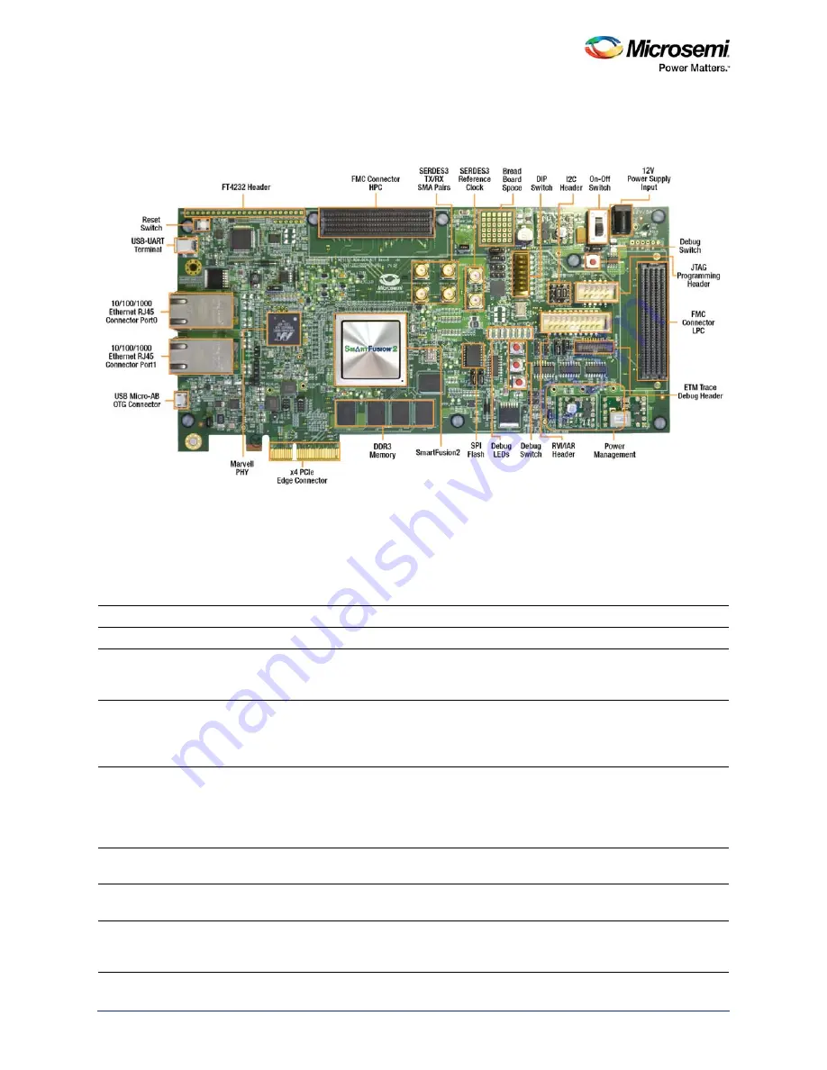
The following figure is a snapshot of the SmartFusion2 Advanced Development Board with its
engineering silicon.
Figure 2 •
SmartFusion2 Advanced Development Board
2.5
Board Key Components
The following table lists key components of the SmartFusion2 Advanced Development Board.
Table 2 •
SmartFusion2 Advanced Development Board Components
Name
Description
SmartFusion2 FPGA
M2S150TS-1FCG1152 FPGA with a hard Cortex-M3 processor.
DDR3 synchronous dynamic random
access memory (SDRAM)
4 × 256 MB (256 MB Micron DDR3 memories MT41K256M8DA-125 IT:K) for
storing data, and 256 MB (1 × 256 MB Micron DDR3 memory
MT41K256M8DA-125 IT:K) for storing ECC bits.
SPI flash
A 1-gigabit SPI flash (Micron N25Q00AA13GSF40G) connected to SPI port 0
of the SmartFusion2 microcontroller subsystem (MSS), and another 1-gigabit
SPI flash (Micron N25Q00AA13GSF40G) connected to the SmartFusion2
fabric.
Ethernet
Two RJ45 connectors (Ethernet jacks with built-in magnetics) interfacing with a
Marvell 10/100/1000 BASE-T physical layer (PHY) chip—88E1304S—in Serial
Gigabit Media Independent Interface (SGMII) mode. The Marvell PHY device,
in turn, interfaces with the Ethernet port of the SmartFusion2 MSS (on-chip
MAC and external PHY).
RVI header
RVI header for application programming and debugging using Keil ULINK or
IAR J-Link.
Embedded FlashPro5
Embedded FlashPro5 for programming and debugging the SmartFusion2
FPGA using Microsemi tools.
Future Technology Devices
International (FTDI) programmer
FTDI programmer interface (J33) to program the external SPI flash. An FTDI
chip is also used to change the JTAG_SEL signal (
high
or
low
) remotely for
switching between the RVI header and JTAG mode.


