


PIC16F716
DS41206A-page 48
Preliminary
2003 Microchip Technology Inc.
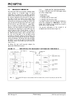
7.4.7
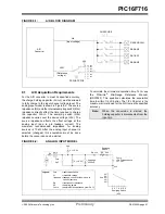
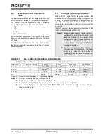
SETUP FOR PWM OPERATION
The following steps should be taken when configuring
the ECCP module for PWM operation:
1.
Configure the PWM pins P1A and P1B (and
P1C and P1D, if used) as inputs by setting the
corresponding TRISB bits.
2.
Set the PWM period by loading the PR2 register.
3.
Configure the ECCP module for the desired
PWM mode and configuration by loading the
CCP1CON register with the appropriate values:
• Select one of the available output
configurations and direction with the
P1M1:P1M0 bits.
• Select the polarities of the PWM output
signals with the CCP1M3:CCP1M0 bits.
4.
Set the PWM duty cycle by loading the CCPR1L
register and CCP1CON<5:4> bits.
5.
For Half-Bridge Output mode, set the dead-
band delay by loading PWM1CON<6:0> with
the appropriate value.
6.
If auto-shutdown operation is required, load the
ECCPAS register.
• Select the auto-shutdown sources using the
ECCPAS<2> AND ECCPAS<0> bits.
• Select the shutdown states of the PWM output
pins using PSSAC1:PSSAC0 and
PSSBD1:PSSBD0 bits.
• Set the ECCPASE bit (ECCPAS<7>).
7.
If auto-restart operation is required, set the
PRSEN bit (PWM1CON<7>).
8.
Configure and start TMR2:
• Clear the TMR2 interrupt flag bit by clearing
the TMR2IF bit (PIR1<1>).
• Set the TMR2 prescale value by loading the
T2CKPSx bits (T2CON<1:0>).
• Enable Timer2 by setting the TMR2ON bit
(T2CON<2>).
9.
Enable PWM outputs after a new PWM cycle
has started:
• Wait until TMR2 overflows (TMR2IF bit is set).
• Enable the CCP1/P1A, P1B, P1C and/or P1D
pin outputs by clearing the respective TRISB
bits.
• Clear the ECCPASE bit (ECCPAS<7>).
See the previous section for additional details.
7.4.8
EFFECTS OF A RESET
Both Power-on and subsequent Resets will force all
ports to Input mode and the ECCP registers to their
Reset states.
This forces the Enhanced CCP module to reset to a
state compatible with the standard ECCP module.
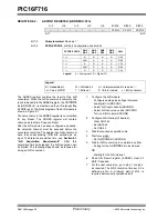
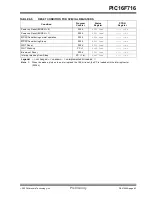
TABLE 7-5:
REGISTERS ASSOCIATED WITH ENHANCED PWM AND TIMER2
Address
Name
Bit 7
Bit 6
Bit 5
Bit 4
Bit 3
Bit 2
Bit 1
Bit 0
Value on
POR, BOR
Value on
all other
Resets
0Bh
INTCON
GIE
PEIE
TMR0IE
INT0IE
RBIE
TMR0IF
INT0IF
RBIF
0000 000x 0000 000u
0Ch
PIR1
—
ADIF
—
—
—
CCP1IF
TMR2IF
TMR1IF
-0-- -000 -0-- -000
8Ch
PIE1
—
ADIE
—
—
—
CCP1IE
TMR2IE
TMR1IE
-0-- --00 -0-- --00
11h
TMR2
Timer2 Module Register
0000 0000 0000 0000
92h
PR2
Timer2 Module Period Register
1111 1111 1111 1111
12h
T2CON
—
TOUTPS3
TOUTPS2
TOUTPS1 TOUTPS0 TMR2ON T2CKPS1 T2CKPS0
-000 0000 -000 0000
86h
TRISB
PORTB Data Direction Register
1111 1111 1111 1111
16h
CCPR1H
Enhanced Capture/Compare/PWM Register1 High Byte
xxxx xxxx uuuu uuuu
15h
CCPR1L
Enhanced Capture/Compare/PWM Register1 Low Byte
xxxx xxxx uuuu uuuu
17h
CCP1CON
P1M1
P1M0
DC1B1
DC1B0
CCP1M3
CCP1M2
CCP1M1
CCP1M0
0000 0000 0000 0000
19h
ECCPAS
ECCPASE
ECCPAS2
—
ECCPAS0
PSSAC1
PSSAC0
PSSBD1
PSSBD0
00-0 0000 00-0 0000
18h
PWM1CON
PRSEN
PDC6
PDC5
PDC4
PDC3
PDC2
PDC1
PDC0
0000 0000 0000 0000
Legend:
x
= unknown,
u
= unchanged,
-
= unimplemented, read as ‘
0
’. Shaded cells are not used by the ECCP module in enhanced PWM mode.
Содержание PIC16F716
Страница 6: ...PIC16F716 DS41206A page 4 Preliminary 2003 Microchip Technology Inc NOTES...
Страница 35: ......
Страница 56: ......
Страница 60: ......
Страница 88: ......
Страница 92: ...PIC16F716 DS41206A page 90 Preliminary 2003 Microchip Technology Inc NOTES...
Страница 108: ...PIC16F716 DS41206A page 106 Preliminary 2003 Microchip Technology Inc NOTES...
Страница 110: ...PIC16F716 DS41206A page 108 Preliminary 2003 Microchip Technology Inc NOTES...
Страница 124: ...PIC16F716 DS41206A page 122 Preliminary 2003 Microchip Technology Inc NOTES...


