


2003 Microchip Technology Inc.
Preliminary
DS41206A-page 19
PIC16F716
3.0
I/O PORTS
Some pins for these I/O ports are multiplexed with an
alternate function for the peripheral features on the
device. In general, when a peripheral is enabled, that
pin may not be used as a general purpose I/O pin.
Additional information on I/O ports may be found in the
PICmicro
®
Mid-Range Reference Manual, (DS33023).
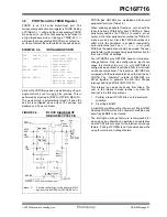
3.1
PORTA and the TRISA Register
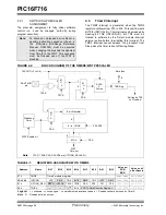
PORTA is a 5-bit wide bidirectional port. The
corresponding data direction register is TRISA. Setting
a TRISA bit (=
1
) will make the corresponding PORTA
pin an input (i.e., put the corresponding output driver in
a High-impedance mode). Clearing a TRISA bit (=
0
)
will make the corresponding PORTA pin an output (i.e.,
put the contents of the output latch on the selected pin).
Reading the PORTA register reads the status of the
pins, whereas writing to it will write to the port latch. All
write operations are read-modify-write operations.
Therefore, a write to a port implies that the port pins are
read, the value is modified and then written to the port
data latch.
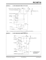
Pin RA4 is multiplexed with the Timer0 module clock
input to become the RA4/T0CKI pin. The RA4/T0CKI
pin is a Schmitt Trigger input and an open drain output.
All other RA port pins have TTL input levels and full
CMOS output drivers.
PORTA pins, RA3:0, are multiplexed with analog inputs
and analog V
REF
input. The operation of each pin is
selected by clearing/setting the control bits in the
ADCON1 register (A/D Control Register 1).
The TRISA register controls the direction of the RA
pins, even when they are being used as analog inputs.
The user must ensure the bits in the TRISA register are
maintained set when using them as analog inputs.
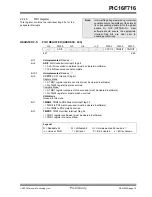
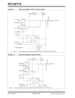
EXAMPLE 3-1:
INITIALIZING PORTA
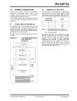
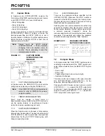
FIGURE 3-1:
BLOCK DIAGRAM OF
RA3:RA0
Note:
On a Power-on Reset, these pins are
configured as analog inputs and read as
‘
0
’.
Note:
Setting RA3:0 to output while in Analog
mode will force pins to output contents of
data latch.
BCF
STATUS, RP0
;
CLRF
PORTA
;Initialize PORTA by
;clearing output
;data latches
BSF
STATUS, RP0
;Select Bank 1
MOVLW
0xEF
;Value used to
;initialize data
;direction
MOVWF
TRISA
;Set RA<3:0> as inputs
;RA<4> as outputs
BCF
STATUS, RP0
;Return to Bank 0
DATA
BUS
Q
D
Q
CK
Q
D
Q
Q
D
EN
P
N
WR
PORT
WR
TRIS
Data Latch
TRIS Latch
RD TRIS
RD PORT
V
SS
V
DD
I/O pin
Analog
Input
mode
TTL
Input
Buffer
To A/D Converter
V
SS
V
DD
CK
Содержание PIC16F716
Страница 6: ...PIC16F716 DS41206A page 4 Preliminary 2003 Microchip Technology Inc NOTES...
Страница 35: ......
Страница 56: ......
Страница 60: ......
Страница 88: ......
Страница 92: ...PIC16F716 DS41206A page 90 Preliminary 2003 Microchip Technology Inc NOTES...
Страница 108: ...PIC16F716 DS41206A page 106 Preliminary 2003 Microchip Technology Inc NOTES...
Страница 110: ...PIC16F716 DS41206A page 108 Preliminary 2003 Microchip Technology Inc NOTES...
Страница 124: ...PIC16F716 DS41206A page 122 Preliminary 2003 Microchip Technology Inc NOTES...


