MDDR Subsystem
Microsemi Proprietary UG0446 User Guide Revision 7.0
17
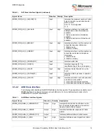
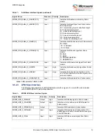
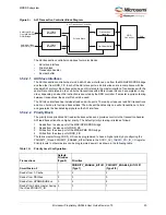
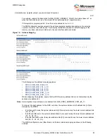
Figure 3 •
Reset Sequence
3.5.3.3
ZQ Calibration
This is applicable for DDR3 only. The ZQ calibration command is used to calibrate DRAM output drivers
(R
ON
) and on-die termination (ODT) values. The DDR3 SDRAM needs a longer time to calibrate R
ON
and ODT at initialization and a relatively smaller time to perform periodic calibrations.
The DDR controller performs ZQ calibration by issuing a ZQ calibration long (ZQCL) command and ZQ
calibration short (ZQCS) command.
ZQCL is used to perform initial calibration during the power-up initialization sequence. This command is
allowed for a period of t
ZQinit
, as specified by memory vendor. The value of t
ZQinit
can be modified
through register bits
The ZQCS command is used to perform periodic calibration to account for voltage and temperature
variations. A shorter timing window is provided to perform calibration and transfer of values as defined by
timing parameter tZQCS. The tZQCS parameter can be modified through register bits
Other activities are not performed by the controller for the duration of t
ZQinit
and tZQCS. All DRAM banks
are precharged and tRP is met before ZQCL or ZQCS commands are issued by the DDR controller.
3.5.3.4
DRAM Training
High Speed DDR3 memories typically requires the DDR controller to implement Write-Leveling, Read
DQS Gate Training, and Read Data Eye Training. However, MDDR only supports a maximum data rate
of 333 MHz/667 Mbps, which means the clock period and data window are relatively large compared to
high-speed DDR3 memory interfaces. Therefore dynamic write-leveling and read training are not
performed. The following sections describe how write-leveling and read training are addressed by the
MDDR.
3.5.3.4.1
Write Leveling
Dynamic write-leveling is not required for the MDDR controller. The board-layout needs to follow
SmartFusion2 and IGLOO2 Board Design Guidelines Application Note
to keep the skew between DQS
and CK within the JEDEC DDR3 tDQSS limit of +/- 750ps at each memory device. For board layouts
which do not meet the Board Design Guidelines, the MDDR controller allows static delay ratios which
delays DQS for each byte lane so that the skew between DQS and CK is kept within JEDEC limits.
333 MHz/667 Mbps is the maximum DDR3 rate MDDR supports. Leveling is not mandatory and the
interface will work if the board layout guidelines are followed and length matching is done.
PO_RESET_N
50 MHz Clock
Enable
Enable I/Os
DDRIO
Calibration
SC_HPMS_RESET_N
(for IGLOO2)
or,
SC_MSS_RESET_N
(for SmartFusion2)
MPLL Lock
MDDR_AXI_RESET_N

