


...........continued
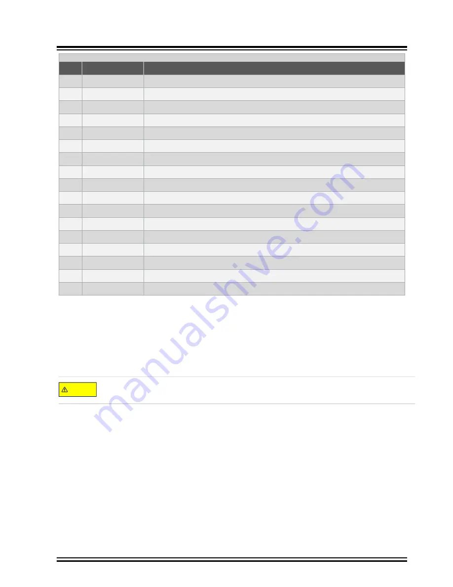
Pin
Signal Name
Signal Description
4
ADC(-)
Analog-to-Digital converter, alternatively negative part of differential ADC
5
GPIO1
General purpose I/O
6
GPIO2
General purpose I/O
7
PWM(+)
Pulse-Width Modulation, alternatively positive part of differential PWM
8
PWM(-)
Pulse-Width Modulation, alternatively negative part of differential PWM
9
IRQ/GPIO
Interrupt request line and/or general purpose I/O
10
SPI_SS_B/ GPIO
Slave B select for SPI and/or general purpose I/O
11
I2C_SDA
Data line for I
2
C interface
12
I2C_SCL
Clock line for I
2
C interface
13
UART_RX
Receiver line of ATtiny817 USART
14
UART_TX
Transmitter line of ATtiny817 USART
15
SPI_SS_A
Slave A select for SPI
16
SPI_MOSI
Master out slave in line of serial peripheral interface
17
SPI_MISO
Master in slave out line of serial peripheral interface
18
SPI_SCK
Clock for serial peripheral interface
19
GND
Ground
20
VCC
Power for extension board
4.3
Current Measurement
The power to the target controller ATtiny817 and its peripherals is connected from the
VCC_BOARD
supply to the
targets
VCC_TARGET
supply with a 0Ω resistor (
R104
), as shown in the figure below. To measure the power
consumption of the device, remove the 0Ω resistor and replace it with an ammeter. The ammeter can be connected
between the
VCC_BOARD
(pin 2 on the target voltage select header) and
VCC_TARGET
(pin 2 on the power
header) pads for easy measurement.
CAUTION
Removing the resistor while the kit is powered without an ammeter or 0Ω resistor mounted may cause the
ATtiny817 to be powered through its I/O pins. This may cause permanent damage to the device.
ATtiny817 Xplained Mini
Hardware User Guide
©
2019 Microchip Technology Inc.
User Guide
DS50002657B-page 15


