background image

64Z8012A

DIFF: 

Op.del.,trip sig.PSx

[   *   ]

DIFF: 

Idiff>(CTS)  PSx

or

if

CTS: 

Idiff>(CTS)active 

= yes

DIFF: 

Sat.discr. 1 trigg.

[ 041 115 ]

DIFF: 

Sat.discr. 2 trigg.

[ 041 116 ]

DIFF: 

Sat.discr. 3 trigg.

[ 041 117 ]

DIFF: 

Harm.block 1 trigg.

[ 041 118 ]
DIFF: 

Harm.block 2 trigg.

[ 041 119 ]
DIFF: 

Harm.block 3 trigg.

[ 041 120 ]

DIFF: 

Overflux.bl.1 trigg.

[ 041 121 ]

DIFF: 

Overflux.bl.2 trigg.

[ 041 122 ]
DIFF: 

Overflux.bl.3 trigg.

[ 041 123 ]

DIFF: 

Enabled

[ 041 210 ]

MAIN: 

Protection active

306 001

DIFF: 

Id,1

303 303

DIFF: 

IR,1

303 305

DIFF: 

Id,2

303 304

DIFF: 

IR,2

303 306

DIFF: 

Id,3

303 307

DIFF: 

IR,3

303 308

DIFF: 

Trip signal

[ 041 075 ]

DIFF: 

Trip signal 1

[ 041 002 ]

DIFF: 

Trip signal 2

[ 041 003 ]

DIFF: 

Trip signal 3

[ 041 004 ]

DIFF: 

Id>> triggered

[ 041 221 ]

DIFF: 

Meas.system 1 trigg.

[ 041 124 ]
DIFF: 

Meas.system 2 trigg.

[ 041 125 ]
DIFF: 

Meas.system 3 trigg.

[ 041 126 ]

DIFF: 

Id>>> triggered

[ 041 222 ]

DIFF: 

Op.mode rush rst.PSx

[   *   ]

DIFF: 

m1  PSx

[   *   ]

DIFF: 

m2  PSx

[   *   ]

DIFF: 

IR,m2  PSx

[   *   ]

DIFF: 

Idiff>>  PSx

[   *   ]

DIFF: 

Idiff>>>  PSx

[   *   ]

0: Without

1: Not phase-selective

2: Phase-selective

DIFF: 

Idiff>  PSx

[   *   ]

[ 036 203 ]

0

1

2

Parameter

set 1
set 2
set 3
set 4

DIFF: 

IR,m2  PSx
072 147
073 147
074 147
075 147

DIFF: 

m2  PSx
072 146
073 146
074 146
075 146

DIFF: 

m1  PSx
072 145
073 145
074 145
075 145

DIFF: 

Idiff>>  PSx
072 143
073 143
074 143
075 143

DIFF: 

Idiff>>>  PSx
072 144
073 144
074 144
075 144

Parameter

set 1
set 2
set 3
set 4

DIFF: 

Idiff>(CTS)  PSx
080 000
081 000
082 000
083 000

DIFF: 

Idiff>  PSx
072 142
073 142
074 142
075 142

DIFF: 

Op.mode rush rst.PSx
072 148
073 148
074 148
075 148

DIFF: 

Op.del.,trip sig.PSx
010 162
010 163
010 164
010 165

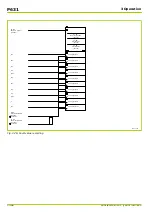
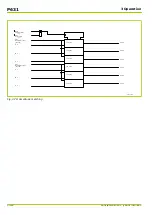
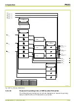
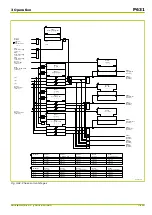
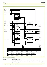
Fig. 3-85: Measuring system of the P631

3.21.7

Inrush Stabilization (Harmonic Restraint)

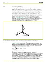
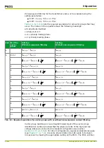
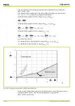
When an unloaded transformer is connected, the inrush current at unfavorable
switching instants such as for voltage zero, may have values that exceed the

P631

3 Operation

3-118

P631/EN M/R-11-C // P631-310-650

Содержание P631

Страница 1: ...MiCOM P631 Transformer Differential Protection Device P631 EN M R 11 C Version P631 310 409 410 650 Technical Manual...

Страница 2: ......

Страница 3: ...on the reference one can navigate directly to the referenced part of the manual In the Adobe Reader or the Acrobat Pro one can return back to the previous view by using the menu point View Page Navig...

Страница 4: ......

Страница 5: ...is P631 The User should be familiar with the warnings in the Safety Guide SFTY 4LM J11 or later version with the warnings in Chapter 5 p 5 1 Chapter 10 p 10 1 Chapter 11 p 11 1 and Chapter 12 p 12 1 a...

Страница 6: ...s or specific problems do not take any action without proper authorization Contact the appropriate technical sales office of Schneider Electric and request the necessary information Any agreements com...

Страница 7: ...Changes after going to press...

Страница 8: ......

Страница 9: ...rent Input 2 12 2 5 5 Resistance Thermometer 2 12 2 5 6 Direct Current Output 2 12 2 5 7 Output Relays 2 13 2 5 8 BCD Measured Data Output 2 13 2 6 Interfaces 2 14 2 6 1 Local Control Panel 2 14 2 6 2...

Страница 10: ...mometer 3 42 3 9 Configuration Operating Mode and Blocking of the Output Relays Function Group OUTP 3 44 3 10 Measured Data Output Function Group MEASO 3 47 3 10 1 General Settings 3 47 3 10 2 BCD Mea...

Страница 11: ...5 3 20 3 Time Tagging 3 105 3 20 4 Fault Recordings 3 106 3 20 5 Fault Value Recording 3 107 3 21 Differential Protection Function Group DIFF 3 109 3 21 1 Enabling or Disabling Differential Protection...

Страница 12: ...158 3 27 2 Assigning Circuit Breakers 3 158 3 27 3 Assigning the Trip Command 3 158 3 27 4 Enabling or Disabling the CBF Function 3 158 3 27 5 Readiness of Circuit Breaker Protection 3 159 3 27 6 Dete...

Страница 13: ...s 6 6 6 5 Menu Tree and Data Points 6 7 6 6 List Data Points 6 8 6 7 Note Concerning the Step by Step Descriptions 6 9 6 8 Configurable Function Keys 6 10 6 8 1 Configuration of the Function Keys F1 t...

Страница 14: ...trol 9 13 9 10 Measurements 9 15 9 11 Configurable Data Attributes 9 16 9 11 1 System LLN0 9 16 10 COMMISSIONING 10 1 10 1 Safety Instructions 10 1 10 2 Commissioning Tests 10 3 10 2 1 Preparation 10...

Страница 15: ...es A3 7 Symbols Used A3 8 A4 TELECONTROL INTERFACES A4 1 A4 1 Telecontrol Interface per EN 60870 5 101 or IEC 870 5 101 Companion Standard A4 1 A4 1 1 Interoperability A4 1 A4 2 Communication Interfac...

Страница 16: ...P631 Table of Contents 8 P631 EN M R 11 C P631 310 650...

Страница 17: ...otection for faults in the CT s secondary circuit Phase swapping allows motor generator protection applications with enlarged protection zones In addition many supplementary protective functions are i...

Страница 18: ...Courier resp via RJ45 or Fiber optics using IEC 61850 16S COMM1 16S COMM2 16E IEC CLK IRIGB CMD_1 SIG_1 26 MEASI MEASO Transformer Differential Protection P631 Always available Optional LIMIT 50 DTOC1...

Страница 19: ...ides a large choice of functions and makes wide ranging application of the protection device possible with just one model version On the other hand simple and clear parameter settings can be made In t...

Страница 20: ...pPhs DtpEft DtpNgsPTCO x DTOCx Definite time overcurrent protection 3 stages phase negative sequence residual starpoint overcurrent 2 51 P Q N ItpPhs ItpEft ItpNgsPTCOx IDMTx Inverse time overcurrent...

Страница 21: ...me synchronization IRIG B 16E IEC Communication interface Ethernet 16E GosGGIOx GOOSE IEC 61850 Measured value functions P631 ANSI IEC 61850 Function group Abbrev Description 26 RtdGGIO1 IdcGGIO1 MEAS...

Страница 22: ...excluded from the configuration Standard Ordering option Inputs and outputs P631 ANSI IEC 61850 Function group Abbrev Description Measuring inputs Phase currents 2 3 INP INP OUTP Binary inputs and ou...

Страница 23: ...event logging MT_RC Monitoring Signal Recording OL_DA Overload Data Acquisition OL_RC Overload recording time tagged event logging FT_DA Fault data acquisition for a particular settable point in time...

Страница 24: ...modular in design The plug in modules are housed in a robust aluminum case and electrically interconnected via one analog p c board and one digital p c board P631 1 Application and Scope 1 8 P631 EN...

Страница 25: ...unction Keys To the right of the text display there are six freely configurable function keys available These may be used for easy control operation access 1 Application and Scope P631 P631 EN M R 11...

Страница 26: ...as per IEC 751 DIN EN 60751 The optional 0 to 20 mA input provides open circuit and overload monitoring zero suppression defined by a setting plus the option of linearizing the input variable via 20 a...

Страница 27: ...hich allow freely configurable function assignment for the colors red and green Furthermore there are various operating modes and flashing functions available PC interface One or two communication int...

Страница 28: ...optionally available with a switchable protocol per IEC 60870 5 103 IEC 870 5 101 DNP 3 0 MODBUS or Courier The second communication interface COMM2 communication protocol per IEC 60870 5 103 only is...

Страница 29: ...oduct designated P631 Transformer Differential Protection Device has been designed and manufactured in conformance with the European standards EN 60255 26 and EN 60255 27 and with the EMC Directive an...

Страница 30: ...nclosed connection area with the supplied rubber grommets fitted Weight Approx 7 kg Dimensions and Connections See dimensional drawings Section 4 2 p 4 4 and the location and terminal connection diagr...

Страница 31: ...n type cable lugs M5 self centering with cage clamp to protect conductor cross sections 4 mm US AWG12 or Threaded terminal ring terminal connection M4 Other inputs and outputs Threaded terminal ends p...

Страница 32: ...V Test generator 50 to 100 M 150 pF 330 Immunity to Radiated Electromagnetic Energy Per EN 61000 4 3 and ENV 50204 severity level 3 Antenna distance to tested device 1 m on all sides Test field streng...

Страница 33: ...ency 5 min Source impedance 12 42 Immunity to Conducted Disturbances Induced by Radio Frequency Fields Per EN 61000 4 6 and EN 60255 22 6 severity level 3 Test voltage 10 V Power Frequency Magnetic Fi...

Страница 34: ...ative humidity and 30 C 86 F with exposure to elevated concentrations of H2S NO2 Cl2 and SO2 2 3 1 4 Mechanical Robustness 1 Applicable to the following case variants Flush mounted case flush mounting...

Страница 35: ...d pulse duration Shock Response tests are carried out to verify full operability during operation test severity class 2 10 g for 11 ms Shock Withstand tests are carried out to verify the endurance dur...

Страница 36: ...Additional Thermal Test 100 controlled thermal endurance test inputs loaded P631 2 Technical Data 2 8 P631 EN M R 11 C P631 310 650...

Страница 37: ...o 55 C 13 F to 131 F Storage and transport 25 C to 70 C 13 F to 158 F Ambient Humidity Range 75 relative humidity annual mean 56 days at 95 relative humidity and 40 C 104 F Condensation not permitted...

Страница 38: ...ing Inputs Nominal current Inom 1 and 5 A AC adjustable Nominal consumption per phase 0 1 VA at Inom Load rating continuous 20 A for 10 s 150 A for 1 s 500 A Nominal surge current 1250 A P631 2 Techni...

Страница 39: ...V DC Special variant 143 V Nominal supply voltage 220 V DC Special variant 163 V Nominal supply voltage 250 V DC Power consumption per input 18 V standard variant VA 19 to 110 V DC 0 5 W 30 VA 110 V...

Страница 40: ...ad monitoring 24 8 mA Zero suppression 0 000 to 0 200 IDC nom adjustable 2 5 5 Resistance Thermometer Only PT 100 permitted for analog I O module mapping curve per IEC 75 1 PT 100 Ni 100 or Ni 120 per...

Страница 41: ...000 W VA at L R 40 ms Breaking capacity 7500 W resistive or 30 A at 250 V DC Maximum values 30 A and 300 V DC 2500 W inductive L R 40 ms or 10 A at 250 V DC Maximum values 10 A and 300 V DC 0 2 A at 2...

Страница 42: ...can only be operated with the interface protocol based on IEC 60870 5 103 Transmission rate 300 or 57600 baud adjustable Wire Leads Per RS 485 or RS 422 2 kV isolation Distance to be bridged Point to...

Страница 43: ...x 100 m Optical Fiber 100 Mbit s Optical wavelength typically 1300 nm ST connector Glass fiber G50 125 Optical output min 18 85 dBm Optical sensitivity min 32 5 dBm Optical input max 12 dBm Glass fibe...

Страница 44: ...2 7 Information Output Counters measured data and indications see chapter Information and Control Functions P631 2 Technical Data 2 16 P631 EN M R 11 C P631 310 650...

Страница 45: ...stabilization or Idiff Idiff 32 ms with inrush stabilization Reset time measured variable from fault infeed to 0 30 ms approx 25 ms 2 8 3 Definite Time and Inverse Time Overcurrent Protection Operate...

Страница 46: ...conditions 2 9 1 2 Differential Protection Measuring system at Idiff 0 2 Iref 10 at Idiff 0 2 Iref 5 Inrush Stabilization Harmonic restraint Deviation 10 2 9 1 3 Restricted Earth Fault Protection Meas...

Страница 47: ...finitions Reference conditions Sinusoidal signals at nominal frequency fnom total harmonic distortion 2 ambient temperature 20 C 68 F and nominal auxiliary voltage VA nom Deviation Deviation relative...

Страница 48: ...urrents measuring inputs 1 Voltages measuring input 0 5 Currents internally calculated 2 Voltages internally calculated 2 Frequency 10 mHz 2 9 3 3 Fault Data Short circuit current and voltage Deviatio...

Страница 49: ...lution 20 sampled values per period 2 10 2 Currents Dynamic range 33 Inom Amplitude resolution at Inom 1 A 2 0 mArms at Inom 5 A 10 1 mArms 2 10 3 Voltage Dynamic range 150 V Amplitude resolution 9 2...

Страница 50: ...events Scope for signals All signals relevant for an overload event from a total of 1024 different logic state signals Depth for signals 200 entries per overload event Ground Fault Memory Number The 8...

Страница 51: ...fault can be set by user 820 periods in total for all faults that is 16 4 s for fnom 50 Hz or 13 7 s for fnom 60 Hz Resolution of the Recorded Data As per Section 2 10 p 2 21 with maximum current dyn...

Страница 52: ...g range for alternating voltage 0 9 to 1 1 VA nom Nominal burden where VA 220 V DC and with maximum module configuration 40 TE case relays de energized energized approx 12 6 W 34 1 W Start up peak cur...

Страница 53: ...uivalent power over the rated resistive burden of the CT for rated secondary current Pbn Rbn Isn 2 Rb Actual resistive burden secondary connected of the CT Pb Equivalent power over the actual resistiv...

Страница 54: ...ven as follows For phase to ground faults Rb 2 Rl Rrel For phase to phase faults Rb Rl Rrel The wire lead burden is calculated as Rl l A specific conductor resistance e g for copper 0 021 mm m 2 1 10...

Страница 55: ...rent sensitivity given by the set basic threshold of the tripping characteristic The empirical dimensioning factor Kemp shown in the diagram above has been determined by investigations using 3 shot au...

Страница 56: ...P631 2 Technical Data 2 28 P631 EN M R 11 C P631 310 650...

Страница 57: ...al binary I O modules X are equipped with optical couplers for binary signal input as well as output relays for the output of signals and commands or combinations of these The external auxiliary volta...

Страница 58: ...spectively a protection communication interface for the transfer of digital information between two protection devices The local control module L is located behind the front panel and connected to the...

Страница 59: ...ols are grouped here for example those for resetting counters memories and displays Events Branch The third branch is reserved for the recording of events All information in this group is therefore st...

Страница 60: ...el is activated as an event occurs the display switches to the appropriate Event Panel provided that measured values have been selected for the Event Panels In the event of overload or ground fault ev...

Страница 61: ...he setting for LOC Hold time for Panels or when the appropriate key on the local control panel is pressed 63Z80CXA LOC Fct Operation Panel 053 007 FT_RC Record in progress 035 000 Measured value 1 Mea...

Страница 62: ...play can accommodate then the display will either switch to the next set of measured fault values at intervals defined by the setting for LOC Hold time for Panels or when the appropriate key on the lo...

Страница 63: ...s at intervals defined by the setting for LOC Hold time for Panels or when the appropriate key on the local control panel is pressed 50Z0140A MAIN Reset LED 306 020 1 execute MAIN General reset EXT 00...

Страница 64: ...signed to the physical communication channels 1 or 2 see Section 3 12 12 p 3 87 If the COMM1 settings have been assigned to communication channel 2 then the settings of communication interface 2 COMM2...

Страница 65: ...t disabled 038 046 MAIN Test mode 037 071 0 No 1 0 1 Yes PC Bay address 003 068 PC Device address 003 069 PC Baud rate 003 081 PC Parity bit 003 181 PC Spontan sig enable 003 187 PC Select spontan sig...

Страница 66: ...standard 1 compatibility level 2 February 1995 edition with additions covering control and monitoring IEC 870 5 101 Telecontrol equipment and systems Part 5 Transmission protocols Section 101 Companio...

Страница 67: ...ILS enable 003 217 1 Yes 0 1 0 No COMM1 MODBUS enable 003 220 1 Yes 0 1 0 No COMM1 DNP3 enable 003 231 1 Yes 0 1 0 No COMM1 COURIER enable 103 040 1 Yes 0 1 0 No COMM1 Communicat protocol 003 167 COMM...

Страница 68: ...r on 003 166 COMM1 Name of manufacturer 003 161 COMM1 Octet address ASDU 003 073 COMM1 Spontan sig enable 003 177 Commun interface COMM1 Sig meas val block 037 075 COMM1 Sig meas block EXT 037 074 MAI...

Страница 69: ...nab cycl dat 003 074 COMM1 Cycl data ILS tel 003 175 COMM1 Line idle state 003 165 COMM1 Baud rate 003 071 COMM1 Delta I 003 051 COMM1 Delta meas v ILS tel 003 150 COMM1 Contin general scan 003 077 CO...

Страница 70: ...l 003 175 COMM1 Delta I 003 051 COMM1 Delta meas v ILS tel 003 150 COMM1 Delta t 003 053 COMM1 Contin general scan 003 077 COMM1 Line idle state 003 165 COMM1 Baud rate 003 071 COMM1 Parity bit 003 17...

Страница 71: ...9 COMM1 MODBUS prot variant 003 214 COMM1 Line idle state 003 165 COMM1 Baud rate 003 071 COMM1 Parity bit 003 171 COMM1 Dead time monitoring 003 176 COMM1 Mon time polling 003 202 COMM1 Octet comm ad...

Страница 72: ...5 COMM1 Baud rate 003 071 COMM1 Parity bit 003 171 COMM1 Dead time monitoring 003 176 COMM1 Mon time polling 003 202 COMM1 Octet comm address 003 072 COMM1 Oct 2 comm addr DNP3 003 240 COMM1 Test moni...

Страница 73: ...M1 Line idle state 003 165 COMM1 Baud rate 003 071 COMM1 Parity bit 003 171 COMM1 Dead time monitoring 003 176 COMM1 Mon time polling 003 202 COMM1 Octet comm address 003 072 COMM1 General enable USER...

Страница 74: ...tart or sig end can then be triggered using setting parameters 48Z50FKA COMM1 Test spont sig end 003 186 Selected signals Signal 1 Signal 2 Signal 3 Signal n 1 execute 0 don t execute 0 1 1 execute 0...

Страница 75: ...IN Test mode 037 071 COMM2 Line idle state 103 165 COMM2 Baud rate 103 071 COMM2 Parity bit 103 171 COMM2 Dead time monitoring 103 176 COMM2 Mon time polling 103 202 COMM2 Octet comm address 103 072 C...

Страница 76: ...via the local control panel 48Z50FLA COMM2 Test spont sig end 103 186 Selected signals Signal 1 Signal 2 Signal 3 Signal n 1 execute 0 don t execute 0 1 1 execute 0 don t execute 0 1 COMM2 Test spont...

Страница 77: ...pecifically created for each device is used as a basis for an exchange of data between the devices and all process control installations interested in such information In order to facilitate engineeri...

Страница 78: ...unication protocol IEC 61850 is available only as an alternative to function group COMM1 3 4 4 1 3 Activating and Enabling The IEC function group can be activated by setting the parameter IEC Function...

Страница 79: ...cd mcl x3v IED Configurator iid IED Configurator PACiS SCE 19Z7001C System configurator Operating program Fig 3 16 Configuration according to IEC 61850 6 3 Operation P631 P631 EN M R 11 C P631 310 650...

Страница 80: ...can supply up to 16 clients linked into the network with spontaneous or cyclic information 3 4 4 1 5 Clock Synchronization With IEC 61850 clock synchronization is effected via the SNTP protocol defin...

Страница 81: ...a buffered transmission which is required for the uninterrupted writing of events A pre defined dataset may be assigned to each report which will then determine which data object will be transmitted...

Страница 82: ...transmission of information the GSSE and the GOOSE The GSSE also named UCA2 GOOSE is used to transmit binary information with a simple configuration by bit pairs and it is compatible with UCA2 The GOO...

Страница 83: ...fore remain in the local network to which the P631 is connected 3 4 4 2 1 Configuration and Enabling Function group GOOSE can be configured by setting the parameter GOOSE Function group GOOSE This par...

Страница 84: ...individual data attributes and not the overlapping data objects By this the amount of data is kept within a limit and decoding is guaranteed on the receiving end In addition to the information includ...

Страница 85: ...ject planning documentation of the sending device or from a configuration file which is conform to IEC 61850 The IED Configurator will support the import of IID SCD and MCL files when the browse funct...

Страница 86: ...condition The state information is reset and accordingly signaled after termination of the command sequence The P631 is capable to monitor the command status of up to 32 further devices With the IED C...

Страница 87: ...h GSSE up to 32 logic binary state signals can be sent Selection of binary state signals is made by setting GSSE Output 1 fct assig or Output 2 Output 32 Each selected state signal is to be assigned t...

Страница 88: ...communications fault the signals received will automatically be set to their respective default value e g GSSE Input 1 default The various settings measured values and signals for function group GOOSE...

Страница 89: ...current date DD MM YY Disabling and Enabling the IRIG B Interface The IRIG B interface can be disabled or enabled using a setting parameter Synchronization Readiness If the IRIG B interface is enable...

Страница 90: ...EXT or LOC Trig menu jmp 2 EXT The functions of the selected menu jump list are triggered in sequence by repeated pressing of the assigned function key Both menu jump lists are assembled at LOC Fct m...

Страница 91: ...ed function F_KEY Fct assignm F1 080 112 F_KEY Operating mode F1 080 132 1 1 F_KEY State F1 080 122 S1 R1 1 0 Keys local control 1 Fig 3 21 Configuration and operating mode of function keys The assign...

Страница 92: ...puts of the analog I O module as these have an increased reaction time due to internal processing In this technical manual it is assumed that the required functions marked EXT in the address descripti...

Страница 93: ...gh 2 Active low filt 3 Active high filt Input signal 0 1 2 3 Function 1 EXT Function 2 EXT Function 3 EXT Function n EXT Activate function Uxxx INP Filter 010 220 INP State U xxx ZZZ ZZZ Fig 3 22 Conf...

Страница 94: ...oned for monitoring purposes IDC lin is also displayed as a measured operating value In addition it is monitored by the Limit Value Monitoring function to detect whether it exceeds or falls below set...

Страница 95: ...in These two setting parameters refer to value pair number 1 setting parameters for value pairs 2 to 20 are available too The resulting points called interpolation points are connected by straight lin...

Страница 96: ..._EN IDC1 IDC2 IDC3 IDC4 IDC20 IDC lin1 IDC lin2 IDC lin3 IDC lin4 IDC lin20 Enable IDC p u Interpolation points Fig 3 25 Example of a characteristic with five interpolation points characteristic with...

Страница 97: ...82 MEASI IDC lin 17 037 183 MEASI IDC 18 037 184 MEASI IDC lin 18 037 185 MEASI IDC 19 037 186 MEASI IDC lin 19 037 187 MEASI IDC 20 037 188 MEASI IDC lin 20 037 189 MEASI Enable IDC p u 037 190 MEASI...

Страница 98: ...ainst overloading If it exceeds the set threshold of 24 8 mA the signal MEASI Overload 20mA input is issued 3 8 2 Input for Connection of a Resistance Thermometer This input is designed to connect a P...

Страница 99: ...I Temperature p u 004 221 MEASI Temperature 004 133 MEASI Temperature Tmax 004 233 MEASI Enabled 035 008 Measur input PT100 C Fig 3 28 Temperature measurement with a resistance thermometer 3 Operation...

Страница 100: ...a new fault signalized by the onset of a general starting or of a new system disturbance Blocking the Output Relays The P631 offers the option of blocking all output relays via a setting parameter or...

Страница 101: ...gnal n SFMON Hardware fault 304 950 OUTP Block outp rel EXT 040 014 MAIN Prot ext disabled 038 046 FT_RC Record in progress 035 000 FT_RC System disturb runn 035 004 MAIN General reset USER 003 002 1...

Страница 102: ...t 003 042 OUTP Hold time for test 003 044 OUTP Fct assignment K xx2 BBB BBB OUTP Fct assignment K xx3 CCC CCC OUTP Fct assignment K xxx ZZZ ZZZ MAIN Device on line 003 030 0 No off K yyy 0 don t execu...

Страница 103: ...r enabled via setting parameters S8Z52H1A MEASI General enable USER 011 100 MEASI Enabled 035 008 1 Yes 0 1 0 No Fig 3 31 Disabling or enabling the measured data output function 3 10 1 2 Enabling Meas...

Страница 104: ...set 037 117 MEASO Reset meas val outp 304 601 0 0 don t execute 1 execute MEASO Reset output USER 037 116 1 MAIN Reset indicat USER 021 010 1 execute MAIN General reset USER 003 002 1 execute MEASO Re...

Страница 105: ...g value that has been output will be stored until the measured data output function is reset 3 10 2 3 Scaling of BCD Output In order to define the resolution for measured data output the measurand ran...

Страница 106: ...in the data model Scaled min val BCD Scaled max val BCD Measurands BCD display values Measurands in the range Measurands to be output BCD Out min value BCD Out max value Valid BCD value Measurands Mx...

Страница 107: ...O 1 digit bit 0 BCD 037 051 MEASO 1 digit bit 1 BCD 037 052 MEASO 1 digit bit 2 BCD 037 053 MEASO 1 digit bit 3 BCD 037 054 MEASO 10 digit bit 0 BCD 037 055 MEASO 10 digit bit 1 BCD 037 056 MEASO 10 d...

Страница 108: ...ction is reset 3 10 3 3 Configuration of Output Relays Assigned to the Output Channels The user must keep in mind that direct current output only occurs when the output relays assigned to the output c...

Страница 109: ...the data model Scal min value Ax Scal knee point Ax Scaled max val Ax 3 10 3 6 Associated Display Range The associated display range is defined by setting the following parameters MEASO AnOut min val...

Страница 110: ...easurands of the variable Mx 0 V 150 V Associated scaled measurands 0 1 Measurands to be output Range Measurands with knee point to be output 2 V 10 V 100 V Associated scaled measurands 0 013 0 067 0...

Страница 111: ...are smaller than or equal to the set minimum measured value to be transmitted The setting at MEASO AnOut max val A 1 defines the output current that is output for the maximum measured value to be tran...

Страница 112: ...Mx scal 0 013 0 067 0 667 Vnom 1 0 19Z5265A Fig 3 35 Example of a characteristic curve for analog measured data output In this example the range starting value is 0 also possible is directional signed...

Страница 113: ...value Selected Meas event value being updated MEASO Scaled min val A 1 037 104 MEASO Scaled knee val A 1 037 105 MEASO Scaled max val A 1 037 106 MEASO AnOut min val A 1 037 107 MEASO AnOut knee point...

Страница 114: ...s interface MEASO Output value 1 MEASO Output value 1 MEASO Output value 1 These external measured values are output by the P631 either in BCD data form or as load independent direct current provided...

Страница 115: ...tional readiness of the P631 supply voltage is present H 17 red EDIT MODE Not configurable H 17 indicates the input edit mode Only when the P631 is in this mode can parameter settings be changed by pr...

Страница 116: ...onfigured binary signal input see Section 3 12 p 3 62 at the onset of a new fault signalized by the onset of a general starting or of a new system disturbance depending on the selected operating mode...

Страница 117: ...reset syst dist 5 NE updating 6 NE manual reset 45Z8000A LED State Hxx red zzz zzz 1 2 3 4 5 6 Hxx red MAIN Reset LED 306 020 7 ES updating bl 8 ES manual reset bl 9 ES reset fault bl 10 ES rst syst d...

Страница 118: ...processing The P631 has the following measuring inputs Current inputs three phases for the processing of measured values for 2 winding ends of the transformer 61Z8001A A B C a b 1IA 1IB 1IC 2IA 2IB 2...

Страница 119: ...a I C a 1IA 1IB 1IC A B C a b A B C Connection Part 1 Fig 3 40 Connection of the measured values to the P631 looping of the fourth current transformer set into the ground connections of the phase cur...

Страница 120: ...AIN Conn meas circ IP b 010 150 I A b I B b I C b P631 Fig 3 41 Connection of the measured values to the P631 looping of the fourth current transformer set into the ground connections of the phase cur...

Страница 121: ...tection functions IDMTx DTOCx as well as Current Transformer Supervision CTS and Measuring Circuit Monitoring MCM_x functions PS1 PS2 PS3 PS4 Description Range of Values 010 200 010 201 010 202 010 20...

Страница 122: ...62Z8002A 1 MAIN Phase reversal a PSx 010 201 010 200 010 202 010 203 MAIN Phase reversal b PSx 010 205 010 204 010 206 010 207 MAIN Phase reversal activ 036 220 Parameter set 1 set 2 set 3 set 4 Param...

Страница 123: ...he transformer Delayed and stored maximum phase current of each end of the transformer Positive and negative sequence current measured values of each end of the transformer Current IN derived by the P...

Страница 124: ...per curve in Fig 3 43 p 3 69 The time after which the delayed maximum phase current display will have reached 95 of maximum phase current IP max is set at MAIN Settl t IP max del Stored Maximum Phase...

Страница 125: ...ax a p u 005 160 MAIN IP max p u stored a 005 163 MAIN IP max p u delay a End b 005 112 MAIN Curr IP max b p u 006 160 MAIN IP max p u stored b 006 163 MAIN IP max p u delay b Fig 3 43 Operation of de...

Страница 126: ...AIN Settl t IP max del 010 113 MAIN Reset IP max st USER 003 033 0 1 0 don t execute 1 execute MAIN General reset USER 003 002 1 execute MAIN Hardware fault 306 018 I A z I B z I C z I max z I min z C...

Страница 127: ...d a End b MAIN Current Ineg a prim 005 125 MAIN Current Ineg b prim 005 129 MAIN Current Ipos a prim 005 127 MAIN Current Ipos b prim 005 134 MAIN Current Ineg a p u 005 126 MAIN Current Ineg b p u 00...

Страница 128: ...AB end a End a End b 005 089 MAIN Angle phi AB end a 005 089 MAIN Angle phi BC end a 006 089 MAIN Angle phi CA end a 007 089 I A z MAIN General starting 036 000 MAIN Hardware fault 306 018 I B z I C z...

Страница 129: ...090 0 033 Inom 0 033 Inom 0 033 Inom 0 033 Inom 0 033 Inom 0 033 Inom I A a MAIN General starting 036 000 MAIN Hardware fault 306 018 I B a I C a I A b I B b I C b Fig 3 47 Determination of the angle...

Страница 130: ...unction to be cancelled If for example the LIMIT function group is to be cancelled the setting of LIMIT Function group LIMIT is set to Without To re include the LIMIT function in the P631 configuratio...

Страница 131: ...n line 003 030 0 1 1 Yes on 0 No off 0 No off MAIN Prot ext enabled 003 028 MAIN Protection active 306 001 MAIN Prot ext disabled 038 046 MAIN Enable protect EXT 003 027 MAIN Disable protect EXT 003 0...

Страница 132: ...rameters via an appropriately configured binary signal input If the hold time is set to 0 s switching is effective as long as the binary signal input is being triggered 64Z8005A MAIN Dynam param activ...

Страница 133: ...ign block 1 021 021 MAIN Blocking 1 EXT 040 060 Function 1 Function 2 Function 3 Selected functions m out of n MAIN Fct assign block 2 021 022 Function 1 Function 2 Function 3 Selected functions m out...

Страница 134: ...ring MCMON function are combined to one signal in function group MAIN 62Z5185A MAIN Meas circ I faulty 036 155 MCM_1 Meas circ I faulty 036 198 SFMON Meas circ I faulty 091 018 MCM_2 Meas circ I fault...

Страница 135: ...MAIN Fct assign fault 021 031 MAIN Protect not ready 004 060 MAIN Blocked faulty 004 065 SFMON Blocking 304 951 Fig 3 52 Blocked Faulty signal 3 12 9 Starting Signals and Tripping Logic 3 12 9 1 Trip...

Страница 136: ...54 Counter for general starting signals 3 12 9 4 Trip Command The P631 has four trip commands The functions to effect a trip can be selected by setting an m out of n parameter independently for each...

Страница 137: ...n MAIN Trip cmd block EXT 036 045 MAIN Man trip cmd EXT 037 018 MAIN Reset latch trip EXT 040 138 Fig 3 55 Forming the trip commands 3 12 9 5 Manual Trip Command A manual trip command may be issued v...

Страница 138: ...p cmds 3 009 056 MAIN No gen trip cmds 4 009 057 MAIN Gen trip command 1 036 071 MAIN General reset USER 003 002 1 execute MAIN Gen trip command 2 036 022 MAIN Gen trip command 3 036 113 MAIN Gen trip...

Страница 139: ...nly Impulse every minute via a binary signal input MAIN see Fig 3 57 p 3 83 and the preceding section A primary and a backup source for time of day synchronization may be set where both provide the fo...

Страница 140: ...mple Assign parameter FT_RC Reset record EXT to the relevant binary signal input e g INP Fct assignm U xxx Group resetting by setting parameters by navigating to menu point MAIN Group reset 1 USER or...

Страница 141: ...05 213 12Z61RMB OP_RC Reset record EXT 005 213 0 1 0 don t execute 1 execute 1 m out of n MAIN Fct assign reset 2 MAIN Group reset 2 USER OP_RC Reset record EXT 005 213 MAIN Group reset 2 EXT Fig 3 59...

Страница 142: ...ot distinct resetting actions but make access especially easy to one of the resetting actions described above i e by configuring them to a configurable key One can include the relevant resetting actio...

Страница 143: ...automatically assigned to communications channel 1 COMM2 can only be used to transmit data to and from the P631 if its PC interface has been de activated As soon as the PC interface is used to transm...

Страница 144: ...test mode so that all incoming signals via the serial interfaces will be identified accordingly D5Z50EBA MAIN Test mode USER 003 012 MAIN Test mode EXT 037 070 0 No 0 1 MAIN Test mode 037 071 1 Yes F...

Страница 145: ...his is only true when only one binary signal input is set to a logic level of 1 If more than one signal input is set to a logic level of 1 then the parameter subset previously selected remains active...

Страница 146: ...ctive 036 090 PSS Actual param subset 003 062 PSS PS 2 active 036 091 PSS PS 3 active 036 092 PSS PS 4 active 036 093 PSS PS 1 activated ext 036 094 PSS Ext sel param subset 003 061 PSS PS 2 activated...

Страница 147: ...nitoring tests will be run during operation In the event of a positive test result a specified monitoring signal will be issued and stored in a non volatile NV memory the monitoring signal memory alon...

Страница 148: ...no setting parameters are affected by the procedure A warm restart can also be triggered manually by control action During a warm restart sequence the protective functions and the communication throu...

Страница 149: ...locking at all so that there would be the danger of maloperation in case of a permanent failure The default for this timer stage is Blocked i e blocking of the protection device with two identical fau...

Страница 150: ...represent a deviation from normal operation such as overloads ground faults or short circuits are also recorded The operating data memory can be cleared reset Counter for Signals Relevant to System Op...

Страница 151: ...itoring signal memory can only be cleared manually by a control action Entries in the monitoring signal memory are not cleared automatically even if the corresponding test in a new test cycle now show...

Страница 152: ...ure Coolant temperature Time remaining before tripping Offset of the thermal replica 3 17 1 Overload Duration In the event of an overload the P631 determines the overload duration The overload duratio...

Страница 153: ...A Coolant temp THRM1 004 157 OL_DA Pre trip t leftTHRM1 004 158 OL_DA Offset THRM1 replica 004 191 64Z5038A OL_RC Reset record USER 100 003 1 execute MAIN General reset USER 003 002 1 execute THRM1 Ob...

Страница 154: ...rd in progress 035 003 OL_RC Reset record EXT 005 241 THRM1 Starting k Iref 039 151 Fig 3 68 Counting overload events 3 18 3 Time Tagging The date of each overload event is stored The overload start o...

Страница 155: ...overload data will also be entered in the overload memory The overload logs can be read from the local control panel or through the PC or communication interfaces 12Z6117A R n 1 2 3 4 5 6 7 8 OL_RC O...

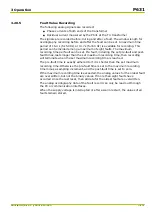
Страница 156: ...the start and end of the FT_RC Record in progress signal 49Z64DMA 1 R FT_DA Running time 004 021 R FT_DA Fault duration 008 010 MAIN General reset USER 003 002 1 execute MAIN Reset LED 306 020 1 MAIN...

Страница 157: ...etween the start of the fault and the fault data acquisition time is determined by the P631 and displayed 61Z8056A FT_DA Run time to meas 004 199 FT_DA Save measured values 305 052 MAIN General reset...

Страница 158: ...sured values 305 052 I B a I C a I A b I B b I C b MAIN General reset USER 003 002 1 execute MAIN Reset LED 306 020 I max a I max b Fig 3 72 Acquisition of the fault currents 3 19 4 Acquisition of the...

Страница 159: ...d in progress 035 000 DIFF Id 2 303 304 DIFF I 2 f0 1 303 301 DIFF IR 1 303 305 DIFF I 5 f0 1 303 311 DIFF I 2 f0 2 303 302 FT_DA Save measured values 305 052 DIFF I 5 f0 2 303 312 DIFF IR 2 303 306 D...

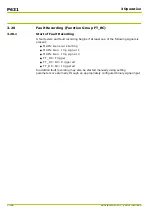
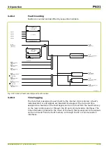
Страница 160: ...ng signals is present MAIN General starting MAIN Gen trip signal 1 MAIN Gen trip signal 2 FT_RC Trigger FT_RC Id triggered FT_RC IR triggered In addition fault recording may also be started manually u...

Страница 161: ...al 2 Signal 3 Signal n Selected signals FT_RC Trigger 037 076 FT_RC Reset record EXT 005 243 0 1 min MAIN General starting 036 000 Fig 3 74 Start of fault recording and fault counter 3 20 3 Time Taggi...

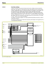
Страница 162: ...In addition to the fault signals the measured RMS fault data will also be entered in the fault memory The fault recordings can be read from the local control panel or through the PC or communication i...

Страница 163: ...ing time then recording will terminate when the set maximum recording time is reached The pre fault time is exactly adhered to if it is shorter than the set maximum recording time Otherwise the pre fa...

Страница 164: ...079 I A a FT_RC Record in progress 035 000 I B a I C a I Y a I P a I A b I B b I C b I Y b I P b V I A c Analog channel 4 Analog channel 5 Analog channel 6 Analog channel 7 Analog channel 8 Analog ch...

Страница 165: ...monic restraint inrush compensation can be deactivated The start up of directly switched asynchronous motors represents a problem in differential protection due to transient transformer saturation cau...

Страница 166: ...ct are then calculated by the P631 on the basis of the set reference power and the set primary nominal voltages of the transformer Iref a Sref 3 Vnom a Iref b Sref 3 Vnom b Sref reference power Iref a...

Страница 167: ...r back to the relevant reference currents rather than to the transformer nominal currents or the nominal currents of the device 62Z8013A kam a 16 kam b 16 SFMON 2nd match fact inv 091 006 DIFF Ref cur...

Страница 168: ...06 001 DIFF Sound match 303 310 DIFF Matching fact kam a 004 105 I A a I B a I C a DIFF Matching fact kam b 004 106 I A b I B b I C b kam a I A a kam a I B a kam a I C a kam b I A b kam b I B b kam b...

Страница 169: ...factor 1 3 the desired matching is achieved Q6Z0105A I am B b I am C b 3 I s 2 b 3 I s 3 b I am A b 3 I s 1 b I am A b I am B b I am C b I s 3 a I s 2 a I s 1 a Fig 3 80 Vector diagram for vector gro...

Страница 170: ...am x 1 b 5 I am x 1 b I am x b 1 3 I am x 1 b I am x b 1 3 I am 0 b 6 I am 0 b I am x b I am x b 7 I am x 1 b I am x b 1 3 I am x 1 b I am x b 1 3 I am 0 b 8 I am x 1 b I am 0 b I am x 1 b 9 I am x 1...

Страница 171: ...aining current values for each measurement system are calculated from the current values after amplitude and vector group matching The following equations are valid for uniformly defined current arrow...

Страница 172: ...ef Idiff Iref 1 0 5 m1 IR m 2 Iref m1 m2 Iref reference current m1 gradient of the characteristic in range 0 5Idiff IR IR m 2 m2 gradient of characteristic in range IR m 2 IR 2 4 6 8 0 2 4 6 8 I III I...

Страница 173: ...table threshold DIFF Idiff PSx the restraining current and the saturation discriminator are no longer taken into account either that is the P631 will trip regardless of the restraining value and the s...

Страница 174: ...041 222 DIFF Op mode rush rst PSx DIFF m1 PSx DIFF m2 PSx DIFF IR m2 PSx DIFF Idiff PSx DIFF Idiff PSx 0 Without 1 Not phase selective 2 Phase selective DIFF Idiff PSx 036 203 0 1 2 Parameter set 1 se...

Страница 175: ...Trip signal 041 075 DIFF Harm block 1 trigg 041 118 I f0 I 2 f0 I 2 f0 I f0 0 30ms DIFF Harm block 2 trigg 041 119 I f0 I 2 f0 I 2 f0 I f0 0 30ms DIFF Harm block 3 trigg 041 120 DIFF I 2 f0 1 303 301...

Страница 176: ...ransformer is loaded with a voltage in excess of the nominal voltage saturation effects occur Without stabilization these could lead to differential protection tripping The fact that the current of th...

Страница 177: ...bl en PSx 0 No 1 Yes 0 1 I 5 f0 I 5 f0 I f0 5 f0 I f0 f0 I 5 f0 5 f0 I f0 f0 I 5 f0 5 f0 I f0 f0 I 5 f0 I f0 I 5 f0 I f0 DIFF Id 1 303 303 DIFF Id 2 303 304 DIFF Id 3 303 307 DIFF Meas system 1 trigg...

Страница 178: ...IFF Restrain current 3 007 081 1 2 3 1 2 3 c1 c2 c3 c1 c2 c3 DIFF Meas value rel Id 011 037 DIFF Meas value rel IR 011 038 DIFF IR 1 303 305 DIFF IR 2 303 306 DIFF IR 3 303 308 DIFF Id 1 303 303 DIFF...

Страница 179: ...he function group DTOC1 will serve as an example to illustrate the operation of the DTOC protection functions The same will apply to function group DTOC2 62Z5070A DTOC1 Select meas input 019 103 0 1 0...

Страница 180: ...threshold types can be active The dynamic thresholds are active for the set hold time for the dynamic parameters see Section 3 12 5 p 3 76 and the normal thresholds are active when no hold time is run...

Страница 181: ...051 078 051 079 051 DTOC1 I dynamic PSx 076 151 077 151 078 151 079 151 DTOC1 tI PSx 076 057 077 057 078 057 079 057 DTOC1 I PSx 076 052 077 052 078 052 079 052 DTOC1 I dynamic PSx 076 152 077 152 078...

Страница 182: ...of two different threshold types can be active The dynamic thresholds are active for the set hold time for the dynamic parameters see Section 3 12 5 p 3 76 and the normal thresholds are active when n...

Страница 183: ...neg 036 153 DTOC1 tIneg elapsed 036 150 DTOC1 Starting Ineg 036 147 DTOC1 Starting Ineg 036 144 DTOC1 Trip signal tIneg 036 151 DTOC1 tIneg elapsed 036 148 DTOC1 Starting Ineg 036 145 DTOC1 Gen starti...

Страница 184: ...tages are started Once the time delays have elapsed a signal is issued If the operating mode of the general starting decision is set to With start IN Ineg a trip signal is issued as well The timer sta...

Страница 185: ...ng A 035 104 DTOC1 Starting B 035 105 DTOC1 Starting C 035 106 2 For multi ph start 2 DTOC1 IN PSx DTOC1 IN dynamic PSx DTOC1 tIN PSx DTOC1 IN PSx DTOC1 IN dynamic PSx DTOC1 tIN PSx DTOC1 IN PSx DTOC1...

Страница 186: ...en starting modePSx 1 0 0 W o start IN Ineg 1 With start IN Ineg DTOC1 tGS PSx DTOC1 Starting Ineg 036 145 DTOC1 Starting Ineg 036 146 DTOC1 Starting Ineg 036 147 DTOC1 Starting N 035 107 DTOC1 Starti...

Страница 187: ...roup IDMT1 will serve as an example to illustrate the operation of the IDMT protection functions The same will apply to function group IDMT2 62Z5027A IDMT1 Select meas input 019 106 0 1 I A y I B y I...

Страница 188: ...1 Enable PSx 081 050 082 050 083 050 084 050 IDMT1 Enabled 038 125 IDMT1 Enable PSx 1 0 0 No 1 Yes 0 0 No 1 Yes IDMT1 General enable USER 031 141 1 Fig 3 98 Enabling or disabling IDMT protection P631...

Страница 189: ...erse 0 14 0 02 2 Very Inverse 13 50 1 00 3 Extremely Inverse 80 00 2 00 4 Long Time Inverse 120 00 1 00 Per IEEE C37 112 t k a I Iref b 1 c tr k R I Iref 2 1 Per ANSI t k a I Iref b 1 c tr k R I Iref...

Страница 190: ...16 17 18 19 20 21 I Iref t s k 0 05 k 0 1 k 1 k 10 0 01 0 1 1 10 100 1000 0 1 2 3 4 5 6 7 8 9 10 11 12 13 14 15 16 17 18 19 20 21 I Iref t s k 0 05 k 0 1 k 1 k 10 IDMT Tripping Characteristics per IEC...

Страница 191: ...1 1 10 100 1000 0 1 2 3 4 5 6 7 8 9 10 11 12 13 14 15 16 17 18 19 20 21 I Iref t s k 0 05 k 0 1 k 1 k 10 0 01 0 1 1 10 100 1000 0 1 2 3 4 5 6 7 8 9 10 11 12 13 14 15 16 17 18 19 20 21 I Iref t s k 0 0...

Страница 192: ...Inverse and RXIDG Type Inverse Characteristic 11 RI Type Inverse 0 01 0 1 1 10 100 1000 0 1 2 3 4 5 6 7 8 9 10 11 12 13 14 15 16 17 18 19 20 21 I Iref t s k 0 05 k 0 1 k 1 k 10 0 01 0 1 1 10 100 1000...

Страница 193: ...further processing Depending on the characteristic selected and the current magnitude the P631 will determine the tripping time Furthermore a minimum tripping time can be set the tripping time will n...

Страница 194: ...teristic P PSx IDMT1 Factor kt P PSx IDMT1 Min trip t P PSx IDMT1 Hold time P PSx IDMT1 Release P PSx Setting IDMT1 Release P PSx 1 Without delay 2 Delayed as per char I P max Iref P IDMT1 Rush restr...

Страница 195: ...o hold time is running The IDMT protection will trigger when the 1 05 fold of the set reference current value is exceeded Dependent on the characteristic selected and the negative sequence current mag...

Страница 196: ...040 090 MAIN Protection active 306 001 I A y I B y I C y IDMT1 Block tIref neg EXT 038 178 1 With start IN Ineg I neg Iref neg IDMT1 Release neg PSx Setting 1 Without delay 2 Delayed as per char I ne...

Страница 197: ...ime will under no circumstances fall below a settable minimum time threshold irrespective of the residual current flow magnitude The inverse time stage can be blocked by an appropriately configured bi...

Страница 198: ...e N PSx Setting 1 IEC Standard Inverse 2 IEC Very Inverse 3 IEC Extr Inverse 4 IEC Long Time Inv 5 IEEE Moderately Inv 6 IEEE Very Inverse 7 IEEE Extremely Inv 8 ANSI Normally Inv 10 ANSI Long Time In...

Страница 199: ...e of a phase current stage Q6Z0131A Parameter set 1 set 2 set 3 set 4 IDMT1 Hold time P PSx 081 055 082 055 083 055 084 055 IDMT1 Starting Iref P 038 110 Case A Case B Per characteristic Non delayed N...

Страница 200: ...Gen starting modePSx 081 059 082 059 083 059 084 059 IDMT1 Starting Iref neg 038 173 IDMT1 General starting 038 115 IDMT1 tGS PSx 081 058 082 058 083 058 084 058 IDMT1 Starting Iref N 038 120 IDMT1 St...

Страница 201: ...Selection of measured values for thermal overload protection 3 24 1 Enabling or Disabling Thermal Overload Protection Thermal overload protection may be enabled or disabled using setting parameters Mo...

Страница 202: ...p set at THRM1 Rel O T trip PSx The accumulated thermal load 0 The updated measured coolant temperature c for the protected object The maximum permissible coolant temperature c max set at THRM1 Max pe...

Страница 203: ...rement of the object temperature 3 24 4 Coolant Temperature Acquisition To permit acquisition of the coolant temperature an analogue I O module Y must be fitted to the P631 If this module is not prese...

Страница 204: ...24 5 Warning Signal A warning signal is issued when the thermal load reaches the warning level set at THRM1 Rel O T warning PSx Moreover a time to tripping threshold pre trip time can be set When the...

Страница 205: ...4 150 THRM1 Trip signal 039 123 THRM1 Warning 039 124 THRM1 Setting error block 039 126 THRM1 Within pre trip time 039 153 SFMON Setting error THRM1 098 038 MAIN Gen trip command 1 036 071 THRM1 Temp...

Страница 206: ...t replica USER 1 0 0 don t execute 1 execute THRM1 Reset replica 039 125 THRM1 Enabled 039 129 THRM1 Reset replica EXT 039 122 Fig 3 115 Resetting the thermal replica P631 3 Operation 3 150 P631 EN M...

Страница 207: ...arately for each parameter subset 0 CTS General enable USER 031 085 1 0 No 0 CTS Enable PSx 1 0 No CTS Enabled 036 080 64Z5300B PSU PS y active Parameter set 1 set 2 set 3 set 4 CTS Enable PSx 001 118...

Страница 208: ...n operate only if a minimum load current is present in the protected object The negative to positive sequence current ratio exceeds a high set threshold value Ineg Ipos in a single winding end In the...

Страница 209: ...1 CTS End a faulty 460 471 CTS End b faulty 460 472 1 1 2 1 Fig 3 119 CTS triggering condition N represents the number of transformer ends that is N 2 a b 3 25 5 Signaling and Indication Triggering o...

Страница 210: ...nder any load condition but protection will remain operational for internal faults with currents exceeding the load current Blocking DIFF Idiff CTS PSx DIFF Idiff PSx In practice differential protecti...

Страница 211: ...132 001 133 1 500 ms 1 execute 1 1 1 460 450 460 472 Fig 3 121 CTS overreaching signals 64Z5305B CTS End a faulty 460 471 t 0 CTS t Latch PSx 1 1 1 S R t 0 CTS t Alarm PSx CTS Alarm end a updat CTS Re...

Страница 212: ...036 194 MCM_1 Enable PSx 1 0 0 No 1 Yes 0 0 No 1 Yes MCM_1 General enable USER 031 146 1 Fig 3 123 Enabling or disabling measuring circuit monitoring 3 26 2 Measuring Circuit Monitoring The negative t...

Страница 213: ...3 124 Measuring circuit monitoring for end a 3 26 3 Multiple Signaling from the Measuring Circuit Monitoring Function The signals issued by the measuring circuit monitoring function and or current tr...

Страница 214: ...n the protected object 3 27 3 Assigning the Trip Command Which of the trip commands is to be used as a start criterion for the respective CBF function may be selected by setting parameters Address Des...

Страница 215: ...55 1 Yes Address Address 1 execute 1 execute Fig 3 126 Enabling or disabling circuit breaker failure protection illustrated for CBF_1 3 27 5 Readiness of Circuit Breaker Protection Circuit breaker fai...

Страница 216: ...ively The CBF function continuously compares sampled current values from the selected end with the set threshold value CBF_1 I As long as current flow criteria are met the phase selective signals CBF_...

Страница 217: ...available The P631 can check the following CB status signals for plausibility and evaluate them The Open signal from the circuit breaker MAIN CB1 open 3p EXT The Closed signal from the circuit breaker...

Страница 218: ...only drop out when a successful opening has been detected from the current flow monitoring or in some cases when the CB signals that its contacts are open 3 27 9 1 Timers and Tripping Logic Associated...

Страница 219: ...cmd blocked 021 013 64Z1104D 0 No CBF_1 Startup 3p 038 211 I B I C CBF_1 Fct assign starting 022 202 Gen trip signal 1 Gen trip signal 2 Gen trip signal 3 Gen trip signal 4 MAIN Gen trip signal 1 036...

Страница 220: ...and t1 038 220 MAIN Latch trip c reset 040 139 CBF_1 Min dur trip cmd t1 022 167 1 1 1 S R MAIN Trip cmd blocked 021 013 CBF_1 Latching trip cmd t1 022 169 0 1 0 No 1 Yes CBF_1 Trip signal t2 038 219...

Страница 221: ...may be triggered by an InterMiCOM teleprotection interface This may also prevent an unwanted triggering of the circuit breaker failure function 19Z6136D CBF_1 Fault behind CB 038 225 CBF_1 Delay faul...

Страница 222: ...CB pos implausible 038 210 MAIN CB1 open 3p EXT 031 028 MAIN CB1 closed 3p EXT 036 051 3 CBF_1 CBsync superv C open 038 229 CBF_1 CBsync superv B open 038 228 CBF_1 CBsync superv A open 038 227 I A I...

Страница 223: ...monitoring function can be disabled or enabled via setting parameters 3 28 2 Monitoring the Linearized Measured DC Values The direct current linearized by the analog measured data input is monitored...

Страница 224: ...C lin 014 113 LIMIT IDC lin 014 114 LIMIT IDC lin 014 115 LIMIT tIDC lin 014 116 LIMIT tIDC lin 014 117 MAIN Protection active 306 001 MEASI Curr IDC lin p u 004 136 t 0 c t 0 c t 0 c t 0 c Fig 3 136...

Страница 225: ...104 LIMIT T 014 105 LIMIT tT 014 107 LIMIT T 014 106 LIMIT tT 014 108 LIMIT tT elapsed 040 172 LIMIT Starting T 040 171 LIMIT tT elapsed 040 173 LIMIT Starting T 040 174 LIMIT tT elapsed 040 176 LIMI...

Страница 226: ...ue monitoring function a setting parameter is provided for this assignment by the user The function will then monitor the minimum and maximum phase currents for the selection If a maximum phase curren...

Страница 227: ..._1 I 015 117 LIM_1 I 015 118 LIM_1 I 015 119 LIM_1 tI 015 120 LIM_1 tI 015 121 LIM_1 tI 015 122 LIM_1 tI 015 123 I A y I B y I C y LIM_1 General enable USER 014 014 MAIN Protection active 306 001 1 Ye...

Страница 228: ...P631 initial conditions for governing the equations can be set using setting parameters through binary signal inputs or through the serial interfaces Logical operations of the function group LOGIC ca...

Страница 229: ...x2 U x3 U xx Address 036 059 LOGIC Set 1 EXT 034 051 LOGIC Reset 1 EXT 034 059 D5Z52FAB Fig 3 140 Control of logic operations via setting parameters or stored input signals The logic does not apply t...

Страница 230: ...don t execute 0 1 LOGIC Trigger 1 034 038 1 execute 0 don t execute 0 1 LOGIC Trigger 8 034 045 1 execute LOGIC Input 1 EXT 034 000 MAIN Protection active 306 001 Signal 1 Signal 2 Signal 3 Signal n L...

Страница 231: ...nce of interlinked Boolean equations The equations are processed in the sequence defined by the order of each equation It should be noted that in the case of overlapping equations the result is provid...

Страница 232: ...the signal parameters are replaced by the corresponding ones from LOG_2 D5Z50BZA LOGIC Output n LOGIC Output n t LOGIC Output n LOGIC Output n t LOGIC Output n LOGIC Output n t t2 0s t1 0s t1 t2 0s t...

Страница 233: ...r LOG_2 if the signal parameters are replaced by the corresponding ones from LOG_2 D5Z50CBA LOGIC Output n LOGIC Output n t LOGIC Output n LOGIC Output n t LOGIC Output n LOGIC Output n t t2 0s t1 0s...

Страница 234: ...ced by the corresponding ones from LOG_2 Through appropriate configuration it is possible to assign the function of a binary input signal to each output of a logic operation The output of the logic op...

Страница 235: ...1 t 044 001 Uxxx Uxxx Signal 1 EXT AAA AAA Signal 2 EXT BBB BBB Signal 3 EXT CCC CCC Signal n EXT NNN NNN LOGIC Output 1 042 032 LOGIC Output 1 t 042 033 Signal 2 EXT BBB BBB Fig 3 148 Signal assignm...

Страница 236: ...P631 3 Operation 3 180 P631 EN M R 11 C P631 310 650...

Страница 237: ...ied degree of IP protection will be maintained In addition to the essential control and display elements a parallel display consisting of multi colored LED indicators is also incorporated see Section...

Страница 238: ...he slots in the left side wall see Fig 4 1 p 4 3 The flush mounted case is connected at the back of the case Warning The local control panel is connected to processor module P by a plug in connecting...

Страница 239: ...mounted case removal of local control panel or in case of a detachable HMI the case front panel The illustration shows the 84TE case with fixed local control panel as an example 4 Design P631 P631 EN...

Страница 240: ...7 5 177 5 184 5 X6 Fig 4 2 Surface mounted 40 TE case Dimensions in mm 227 9 253 6 177 5 213 4 203 0 155 4 5 0 181 3 159 0 168 0 5 0 X6 Fig 4 3 Flush mounted case 40 TE with panel opening flush mount...

Страница 241: ...h mount method 2 with angle brackets and frame Dimensions in mm The device has increased mechanical robustness if flush mount method 2 with angle brackets and frame is used for the flush mounted case...

Страница 242: ...206 0 20 7 46 3 177 5 197 5 3 0 181 3 148 0 168 0 107 3 192 5 X6 Fig 4 6 Detachable HMI with panel opening P631 4 Design 4 6 P631 EN M R 11 C P631 310 650...

Страница 243: ...are modules The following table gives an overview of the modules relevant for the P631 Key standard equipment optional depending on order Module is not depicted in the terminal connection diagrams Sec...

Страница 244: ...ant Ethernet Board 100 Mbit s DHP Protocol glass fiber ST connector 4TE B 000336187 D ff Bus module digital for 40 TE device 4TE B 000337870 D ff Bus module analog 4TE L 009651473 C ff Local control m...

Страница 245: ...TE V 4I 8O 009651549 B ff Power supply module 60 250 V DC 100 230 V AC switching threshold 155 V 4TE V 4I 8O 009651548 B ff Power supply module 60 250 V DC 100 230 V AC switching threshold 146 V 4TE X...

Страница 246: ...P631 4 Design 4 10 P631 EN M R 11 C P631 310 650...

Страница 247: ...conductor terminal Fig 5 8 p 5 11 If a cable screen is added to this connection or removed from it then the protective grounding should be checked again Warning The SC connector and RJ45 wire of the E...

Страница 248: ...evision level of each module included in the device when shipped can be determined from the list of components assembly list This list of components should be filed carefully After unpacking each devi...

Страница 249: ...l and a second label can be found on the inside of the device Another copy of the type identification label is fixed to the outside of the P631 packaging Fig 5 1 Example of the type identification lab...

Страница 250: ...air The ambient air must not be significantly polluted by dust smoke gases or vapors or salt Solar Radiation Direct solar radiation on the front of the device must be avoided to ensure that the LC Dis...

Страница 251: ...given in Chapter Design When the P631 is mounted on a cabinet door special sealing measures are necessary to provide the degree of protection required for the cabinet IP 51 Connection of protective gr...

Страница 252: ...cal control panel or front element is connected to processor module P by a plug in connecting cable Make sure the connector position is correct Do not bend the connecting cable Then remove the lower M...

Страница 253: ...se or for the flush mounted case flush mount method 2 with angle brackets and frame see Fig 5 5 p 5 8 is used Connection of protective grounding conductor See Section 5 5 p 5 11 For flush mount method...

Страница 254: ...e The cover frame width of the 40 TE surface mounted case is 280 mm of the 84 TE case is 486 mm The cover frame height is for all cases 204 mm Warning The P631 has increased mechanical robustness if e...

Страница 255: ...or example or an empty sub rack with a blank front panel Fit the 19 mounting rack to a cabinet as shown in Fig 5 7 p 5 10 61Y5077A Tapped bush Connection flange Bolt Fig 5 6 Combining 40 TE flush moun...

Страница 256: ...e Rack frame Fig 5 7 Installing the P631 in a cabinet with a 19 mounting rack Warning Connection of protective grounding conductor See Section 5 5 p 5 11 P631 5 Installation and Connection 5 10 P631 E...

Страница 257: ...also conform to applicable national standards A minimum cross section of 1 5 mm US AWG14 or thicker is required If a detachable HMI is installed a further protective conductor ground earth of at least...

Страница 258: ...he common potential of the grouped connections 5 6 1 Connecting Measuring and Auxiliary Circuits 5 6 1 1 Power Supply Before connecting the auxiliary voltage VA for the P631 power supply it must be en...

Страница 259: ...61Z5084A A B C A B C 1IA 1IB 1IC 2IA 2IB 2IC 2IN a b 1IN P631 Fig 5 9 Standard schematic connection diagram for the P631 5 Installation and Connection P631 P631 EN M R 11 C P631 310 650 5 13...

Страница 260: ...his is to be understood as a recommendation only Connection to binary inputs can be made as desired 5 6 2 Connecting the IRIG B Interface An IRIG B interface for time synchronization may be installed...

Страница 261: ...o a 2 wire communications link is also possible A cable with two symmetrical twisted pair wires is required for a 4 wire data link A 2 wire data link is shown in Fig 5 11 p 5 16 and a 4 wire data link...

Страница 262: ...r number see Chapter Accessories and Spare Parts 19Z6480A First participant connect to the line e g the master Last participant connect to the line Device with half duplex interface P631 P631 XXXX XXX...

Страница 263: ...he master XXXX Last participant connect to the line D1 T D2 R X10 P631 200 220 D1 T D2 R Device with half duplex interface P631 XXXX X10 D1 T D2 R D1 T D2 R Fig 5 12 4 wire data link 5 Installation an...

Страница 264: ...1 P 02 02 A CH1 CH2 A ETH CH2 A Red ETH CH2 03 03 T 6J 04 04 05 05 06 06 07 07 X 4H X 6O 08 08 09 09 V 4I 8O 10 10 Each of the numbered slots can be fitted with max 1 module If a location diagram show...

Страница 265: ...X_2 2 3 K_01 4H K_02 K_04 K_03 Binary module X11 1 X8 1 Type A Serial Channel 1 optical fiber link Per order IRIG B time synchronization Serial Channel 2 wire link only or wire link X Y D2 R X10 1 2...

Страница 266: ...P631 5 Installation and Connection 5 20 P631 EN M R 11 C P631 310 650...

Страница 267: ...panel Controlling switchgear units Readout and modification of settings Readout of cyclically updated measured operating data and logic status signals Readout of operating data logs and of monitoring...

Страница 268: ...Fig 6 1 View of the local control panel and layout of the LED indicators for the text display 6 2 2 Display Illumination If none of the control keys are pressed the display illumination will switch of...

Страница 269: ...Press the left and right keys to navigate through the menu tree in a horizontal direction If the unit is in input mode the left and right keys have a different function Input mode Settings can only b...

Страница 270: ...2 4 5 READ Key Press the READ key to access a selected event recording from either the Panel level or from any other point in the menu tree 6 2 4 6 Configurable Function Keys By pressing a function ke...

Страница 271: ...uick overview of the current state of the bay The menu tree level below the panel level allows the user to select all data points settings signals measured variables etc and to change them if appropri...

Страница 272: ...ons are actually available The Operation Panel is always provided Menu tree Device type Parameters Device ID Configuration parameters Function parameters Global Main functions Parameter subset 1 Param...

Страница 273: ...the menu tree that is active as selected by the user The data points are found at the lowest level of a menu tree branch and they are displayed either with their plain text description or in numerica...

Страница 274: ...ogic functions and event logs When a list data point is selected the symbol is displayed in the bottom line of the LCD indicating that a sub level is situated below this displayed level The individual...

Страница 275: ...ase by pressing keys A small black square to the right of the enter key indicates that the LED indicator labeled Edit Mode is illuminated The examples used here are not necessarily valid for the devic...

Страница 276: ...6 8 Configurable Function Keys P631 6 Local Control HMI 6 10 P631 EN M R 11 C P631 310 650...

Страница 277: ...e the function key It is assumed for the following operating example that function key F1 is enabled only after the password as assigned at F_KEY Password funct key 1 has been entered After the passwo...

Страница 278: ...column Now press the ENTER key If the correct password has been entered the active display will re appear Function key F1 is now effective for the set return time By default no password is required an...

Страница 279: ...kV Step 4 When function keys are pressed during their associated return time then the set function is carried out directly i e without checking for the password again By default i e no password requi...

Страница 280: ...the up key first and release it last in order to avoid unintentional resetting of stored data Voltage A B prim 20 7 kV Voltage B C prim 20 6 kV Jumping from Panel Level to Menu Tree Level Control Ste...

Страница 281: ...p according to system conditions If for example the device detects an overload or a ground fault then the corresponding Measured Value Panel will be displayed as long as the overload or ground fault s...

Страница 282: ...vels follow so that the entire folder structure consists of three main branches and a maximum of three folder levels At the end of each branch of folders are the various function groups in which the i...

Страница 283: ...ided by the menu tree The active branch of the menu tree is displayed in plain text in both modes In the following examples the display is shown in plain text mode only Control Step Description Contro...

Страница 284: ...e change can only be made after the password has been entered Thereafter all further changes with the exception of specially protected control actions see Section 6 11 8 p 6 29 are enabled without ent...

Страница 285: ...Step 1 appears Oper CtrlTest LOC Param change enabl No Step 3 Change the setting to Yes Oper CtrlTest LOC Param change enabl Yes Step 4 Press the enter key again The LED indicator will go out The unit...

Страница 286: ...For some settings it is also necessary to disable the protective function MAIN Device on line menu tree Par Func Glob MAIN Such settings include the configuration settings by means of which the device...

Страница 287: ...to the left or right Par Conf LOC Autom return time 5000 0 s Step 4 Change the value highlighted by the cursor by pressing the up and down keys In the meantime the device will continue to operate with...

Страница 288: ...by an OR operator Other operators NOT OR AND NOT OR and NOT AND are available in the LOGIC function group for linking the selected list items In this way binary signals and binary input signals can b...

Страница 289: ...Par Func Glob MAIN Fct assign trip cmd 02 DIST Trip zone 2 Step 4 Scroll through the assignable functions by pressing the right and left keys in the input mode Par Func Glob MAIN Fct assign trip cmd 0...

Страница 290: ...List Parameter If MAIN Without function is assigned to a given item then all the following items are deleted If this occurs for item 01 everything is deleted P631 6 Local Control HMI 6 24 P631 EN M R...

Страница 291: ...or disabling of a device function A maximum of 100 entries is possible after which the oldest entry is overwritten Control Step Description Control Action Display Step 0 Select the entry point for the...

Страница 292: ...ve been entered since the last reset the overflow signal is displayed as the last entry Mon signal record 01 01 13 10 01 SFMON Exception oper syst Step 3 Press the left key to display the previous ent...

Страница 293: ...eset Fault recording 1 FT_RC Event 22 Step 2 Press the right key repeatedly to see first the measured fault data and then the binary signals in chronological order The time shown in the second line is...

Страница 294: ...be found in section Resetting Actions in Chapter Operation Resetting a single memory from the local control panel is described in the following with the example of a fault memory In this example the...

Страница 295: ...en activated see section Change Enabling Function This setup is designed to prevent accidental output and applies even when the global change enabling function has been activated The password consists...

Страница 296: ...Oper CtrlTest MAIN Man trip cmd USER Don t execute Now press the enter key The LED indicator labeled EDIT MODE will light up This indicates that the setting can now be changed by pressing the up or do...

Страница 297: ...ithin a specific time interval The left right up and down keys may be used to define the password and represent the numbers 1 2 3 and 4 respectively 1 3 4 2 The password can be changed by the user at...

Страница 298: ...d Step 3 Now press the enter key The LED indicator labeled EDIT MODE will light up The third line shows an underscore character _ as the prompt for entering a new password Par Conf LOC Password _ Step...

Страница 299: ...word _ Step 8 The change in password can be canceled at any time before Step 7 by pressing the CLEAR key If this is done the original Password continues to be valid Par Conf LOC Password 6 11 9 2 Loca...

Страница 300: ...Action Display Step 0 Turn off the device Step 1 Turn the device on again At the very beginning of device startup press the four directional keys left right up and down at the same time and hold them...

Страница 301: ...er or the following chapter These parameters are described in Chapter IEC 61850 Settings via IED Configurator Cancelling a Protection or Control Function The user can adapt the device to the requireme...

Страница 302: ...or as signal relays It is important to note that the contact rating of the binary I O modules X varies see Chapter Technical Data One signal can also be assigned simultaneously to several output relay...

Страница 303: ...evice Identification The device identification settings are used to record the ordering information and the design version of the P631 They have no effect on the device functions These settings should...

Страница 304: ...s display cannot be altered spacer DVICE DM IEC 61850 version 002 059 Not measured 0 65535 spacer Software version of the communication software based on the device s protocol per IEC 61850 This displ...

Страница 305: ...DVICE Order ext No 5 000 007 0 0 999 spacer DVICE Order ext No 6 000 008 0 0 999 spacer DVICE Order ext No 7 000 009 0 0 999 spacer DVICE Order ext No 8 000 010 0 0 999 spacer DVICE Order ext No 9 000...

Страница 306: ...r DVICE Order ext No 25 000 027 0 0 999 spacer DVICE Order ext No 26 000 028 0 0 999 spacer DVICE Order ext No 27 000 029 0 0 999 spacer Order extension numbers for the device spacer DVICE Module var...

Страница 307: ...pacer DVICE Module vers slot 4 086 196 27 Not fitted spacer DVICE Module vers slot 5 086 197 27 Not fitted spacer DVICE Module vers slot 6 086 198 27 Not fitted spacer DVICE Module vers slot 7 086 199...

Страница 308: ...itted spacer Index letter specifying the version of the digital bus module B spacer DVICE Variant module B a 086 046 65535 Not fitted spacer Item number of the analog bus module B in this design versi...

Страница 309: ...g and setting Further instructions on this setting are given in the description of the respective operating program spacer DVICE Substation ID 000 036 0 0 9999 spacer ID code for use by the PC program...

Страница 310: ...on OS 002 101 Not measured 0 00 655 35 spacer DVICE SW version OS DM 002 111 1 01 0 00 655 35 spacer DVICE SW version FPGA 010 169 Not measured 0 00 655 35 spacer Internal software version numbers Par...

Страница 311: ...ey is pressed spacer LOC Fct read key 080 110 060 000 MAIN Without function spacer Selection of up to 16 functions to be triggered when pressing the read key Event counters and event recordings are of...

Страница 312: ...t if more values are selected than can be shown on the LC Display spacer LOC Autom return time 003 014 60 60 60000 s Fig 3 2 p 3 5 spacer If the user does not press a key on the local control panel du...

Страница 313: ...Without function Fig 3 5 p 3 9 spacer Selection of spontaneous signals for transmission via the PC interface spacer PC Transm enab cycl dat 003 084 0 Without Fig 3 5 p 3 9 spacer Enable for the cyclic...

Страница 314: ...odel addresses PC IP address PC IP address 1 PC IP address 2 PC IP address 3 Note This interface can only be used if it has been configured PC IP address PC Subnet mask PC IP address mode and activate...

Страница 315: ...m Fig 3 5 p 3 9 spacer The measured frequency value is transmitted via the PC interface if it differs by the set delta from the last measured value transmitted spacer PC Delta meas v ILS tel 003 155 3...

Страница 316: ...M1 Addit 101 enable 003 216 0 No Fig 3 6 p 3 11 spacer Enabling additional settings that are relevant for the protocol based on IEC 870 5 101 spacer COMM1 Addit ILS enable 003 217 0 No Fig 3 6 p 3 11...

Страница 317: ...er COMM1 Line idle state 003 165 1 Light on high Fig 3 7 p 3 12 Fig 3 8 p 3 13 Fig 3 9 p 3 14 Fig 3 10 p 3 15 Fig 3 11 p 3 16 Fig 3 12 p 3 17 spacer Setting for the line idle state indication spacer C...

Страница 318: ...unication master must be less than the time set here spacer COMM1 Octet comm address 003 072 1 0 254 Fig 3 7 p 3 12 Fig 3 8 p 3 13 Fig 3 9 p 3 14 Fig 3 10 p 3 15 Fig 3 11 p 3 16 Fig 3 12 p 3 17 spacer...

Страница 319: ...Setting for the name of the manufacturer Note This setting can be changed to ensure compatibility This setting is hidden unless an IEC 870 5 protocol is enabled spacer COMM1 Octet address ASDU 003 07...

Страница 320: ...tion of the measured values that are transmitted in a user defined telegram via the communication interface Note This setting is hidden unless an IEC 870 5 protocol is enabled spacer COMM1 Delta I 003...

Страница 321: ...minimum time difference between two telegrams Note This setting is hidden unless an IEC 870 5 protocol is enabled spacer COMM1 Comm address length 003 201 1 1 2 Byte Fig 3 8 p 3 13 spacer Setting for...

Страница 322: ...ig 3 8 p 3 13 spacer Setting specifying whether information numbers and function type shall be reversed in the object address Note This setting is hidden unless the IEC 870 5 101 protocol is set space...

Страница 323: ...OMM1 Reg asg selec cmds 003 210 060 000 MAIN Without function Fig 3 10 p 3 15 spacer MODBUS registers in the range 00301 to 00400 are assigned to the selected commands Assignment is made in the order...

Страница 324: ...deleted from the event queue Note This setting is hidden unless the MODBUS protocol is enabled spacer COMM1 Phys Charact Delay 003 241 0 0 254 Bit Fig 3 11 p 3 16 spacer Number of bits that must pass...

Страница 325: ...es for object 1 binary inputs Assignment of indices is made in the order of selection beginning with 0 Note This setting is hidden unless the DNP 3 0 protocol is enabled spacer COMM1 Ind cl bin output...

Страница 326: ...less the COURIER protocol is enabled spacer COMM1 Signal selection 103 043 060 000 MAIN Without function Fig 3 12 p 3 17 spacer Selection of signals to be transmitted via the COURIER protocol Note Thi...

Страница 327: ...face spacer COMM2 Parity bit 103 171 2 Even Fig 3 14 p 3 19 spacer Set the same parity that is set at the interface of the control system connected to the P631 spacer COMM2 Dead time monitoring 103 17...

Страница 328: ...ata Unit spacer COMM2 Spontan sig enable 103 177 0 None Fig 3 14 p 3 19 spacer Enable for the transmission of spontaneous signals via the communication interface spacer COMM2 Select spontan sig 103 17...

Страница 329: ...ication interface if it differs by the set delta quantity from the last measured value transmitted spacer COMM2 Delta meas v ILS tel 103 150 3 0 0 0 15 0 Fig 3 14 p 3 19 spacer The telegram is transmi...

Страница 330: ...unction group IEC spacer IEC Switch Config Bank 104 043 0 don t execute spacer This parameter can only be sent individually Accepting the previously set communication parameters as the active communic...

Страница 331: ...defines which part of the IP address is addressed by the sub network and which part by the device that is logged on to the network Note This is an information parameter read only and its value is set...

Страница 332: ...cer IEC Dayl sav time st d 104 221 7 Sunday spacer IEC Dayl sav time st m 104 222 3 March spacer These three parameters define the date e g at what day of the year for switching from standard time ove...

Страница 333: ...00 104 228 180 0 1440 min spacer This parameter defines the date and time of day for the clock changeover from daylight saving time to standard time The setting is similar to that for the clock chang...

Страница 334: ...fct assig 106 011 060 000 MAIN Without function spacer GOOSE Output 2 fct assig 106 013 060 000 MAIN Without function spacer GOOSE Output 3 fct assig 106 015 060 000 MAIN Without function spacer GOOS...

Страница 335: ...r GOOSE Output 21 fct assig 106 051 060 000 MAIN Without function spacer GOOSE Output 22 fct assig 106 053 060 000 MAIN Without function spacer GOOSE Output 23 fct assig 106 055 060 000 MAIN Without f...

Страница 336: ...N Without function spacer GOOSE Input 6 fct assig 107 056 061 000 MAIN Without function spacer GOOSE Input 7 fct assig 107 066 061 000 MAIN Without function spacer GOOSE Input 8 fct assig 107 076 061...

Страница 337: ...r GOOSE Input 26 fct assig 107 166 061 000 MAIN Without function spacer GOOSE Input 27 fct assig 107 167 061 000 MAIN Without function spacer GOOSE Input 28 fct assig 107 168 061 000 MAIN Without func...

Страница 338: ...1 ms The repetitions counter N will be restarted at count 1 after each state change of a GSSE bit pair spacer GSSE Max cycle 104 053 1 1 60 s spacer Maximum value for the GSSE repetition cycle time in...

Страница 339: ...0 No selection spacer GSSE Output 10 bit pair 104 128 0 No selection spacer GSSE Output 11 bit pair 104 131 0 No selection spacer GSSE Output 12 bit pair 104 134 0 No selection spacer GSSE Output 13...

Страница 340: ...selection spacer GSSE Output 31 bit pair 104 191 0 No selection spacer GSSE Output 32 bit pair 104 194 0 No selection spacer Setting with which GSSE bit pair the configured binary signal of the virtua...

Страница 341: ...GSSE Output 14 fct assig 104 141 060 000 MAIN Without function spacer GSSE Output 15 fct assig 104 144 060 000 MAIN Without function spacer GSSE Output 16 fct assig 104 147 060 000 MAIN Without funct...

Страница 342: ...GSSE Output 32 fct assig 104 195 060 000 MAIN Without function spacer Function assignment of a binary logical state signal to the virtual GSSE outputs The signal configured here is sent through the GS...

Страница 343: ...05 081 0 No selection spacer GSSE Input 18 bit pair 105 086 0 No selection spacer GSSE Input 19 bit pair 105 091 0 No selection spacer GSSE Input 20 bit pair 105 096 0 No selection spacer GSSE Input 2...

Страница 344: ...1 IED name 105 002 1 Remote IED spacer GSSE Input 2 IED name 105 007 1 Remote IED spacer GSSE Input 3 IED name 105 012 1 Remote IED spacer GSSE Input 4 IED name 105 017 1 Remote IED spacer GSSE Input...

Страница 345: ...pacer GSSE Input 21 IED name 105 102 1 Remote IED spacer GSSE Input 22 IED name 105 107 1 Remote IED spacer GSSE Input 23 IED name 105 112 1 Remote IED spacer GSSE Input 24 IED name 105 117 1 Remote I...

Страница 346: ...default 105 023 0 0 spacer GSSE Input 6 default 105 028 0 0 spacer GSSE Input 7 default 105 033 0 0 spacer GSSE Input 8 default 105 038 0 0 spacer GSSE Input 9 default 105 043 0 0 spacer GSSE Input 1...

Страница 347: ...pacer GSSE Input 28 default 105 138 0 0 spacer GSSE Input 29 default 105 143 0 0 spacer GSSE Input 30 default 105 148 0 0 spacer GSSE Input 31 default 105 153 0 0 spacer GSSE Input 32 default 105 158...

Страница 348: ...GSSE Input 11 fct assig 105 054 061 000 MAIN Without function spacer GSSE Input 12 fct assig 105 059 061 000 MAIN Without function spacer GSSE Input 13 fct assig 105 064 061 000 MAIN Without function...

Страница 349: ...t 31 fct assig 105 154 061 000 MAIN Without function spacer GSSE Input 32 fct assig 105 159 061 000 MAIN Without function spacer Function assignment of the virtual GSSE input to a binary logical state...

Страница 350: ...000 MAIN Without function spacer F_KEY Fct assignm F3 080 114 061 000 MAIN Without function spacer F_KEY Fct assignm F4 080 115 061 000 MAIN Without function spacer F_KEY Fct assignm F5 080 116 061 00...

Страница 351: ...Choice between operation of the function key as a key or switch spacer F_KEY Return time fct keys 003 037 10 1 60000 s spacer Once the password has been entered the function keys remain active for no...

Страница 352: ...U 704 152 118 061 000 MAIN Without function spacer INP Fct assignm U 705 152 121 061 000 MAIN Without function spacer INP Fct assignm U 706 152 124 061 000 MAIN Without function spacer INP Fct assignm...

Страница 353: ...acer INP Oper mode U 901 152 146 1 Active high spacer INP Oper mode U 902 152 149 1 Active high spacer INP Oper mode U 903 152 152 1 Active high spacer INP Oper mode U 904 152 155 1 Active high spacer...

Страница 354: ...10 0 mA Fig 3 26 p 3 41 spacer If the input current falls below the set threshold the P631 will issue an open circuit signal spacer MEASI IDC 1 037 150 0 000 0 000 1 200 IDC nom Fig 3 26 p 3 41 spacer...

Страница 355: ...0 000 1 200 IDC nom Fig 3 26 p 3 41 spacer MEASI IDC 20 037 188 1 200 0 000 1 200 IDC nom Fig 3 26 p 3 41 spacer Setting for the input current that will correspond to a linearized value that has been...

Страница 356: ...spacer MEASI IDC lin 16 037 181 Blocked 0 000 1 200 IDC nom Fig 3 26 p 3 41 spacer MEASI IDC lin 17 037 183 Blocked 0 000 1 200 IDC nom Fig 3 26 p 3 41 spacer MEASI IDC lin 18 037 185 Blocked 0 000 1...

Страница 357: ...t assignm K 902 150 196 060 000 MAIN Without function spacer OUTP Fct assignm K 903 150 199 060 000 MAIN Without function spacer OUTP Fct assignm K 904 150 202 060 000 MAIN Without function spacer OUT...

Страница 358: ...02 150 197 1 ES updating spacer OUTP Oper mode K 903 150 200 1 ES updating spacer OUTP Oper mode K 904 150 203 1 ES updating spacer OUTP Oper mode K 905 150 206 1 ES updating spacer OUTP Oper mode K 9...

Страница 359: ...SO General enable USER 031 074 0 No spacer Disabling or enabling the measured data output function spacer MEASO Fct assignm BCD 053 002 060 000 MAIN Without function Fig 3 34 p 3 51 spacer Selection o...

Страница 360: ...ued range BCD Out min value BCD Out max value BBCD display values for measured values Mx min range BCD Out min value BCD display values for measured values Mx max range BCD Out max value spacer MEASO...

Страница 361: ...d values to be output Mx scal min Mx scal max Designation of the set values in the data model Scaled min val Ax Scaled max val Ax with Mx scal min Mx min Mx RL1 Mx RL2 Mx RL1 Mx scal max Mx max Mx RL1...

Страница 362: ...n val Ax Output current to be set for measured values Mx max designation in the data model An Out max val Ax Output current to be set for measured values Mx knee designation in the data model AnOut kn...

Страница 363: ...5 007 036 251 MAIN Gen trip signal spacer LED Fct assig H 4 green 085 057 060 000 MAIN Without function spacer LED Fct assig H 5 red 085 010 060 000 MAIN Without function spacer LED Fct assig H 5 gree...

Страница 364: ...spacer LED Fct assig H14 red 085 037 060 000 MAIN Without function spacer LED Fct assig H14 green 085 087 060 000 MAIN Without function spacer LED Fct assig H15 red 085 040 060 000 MAIN Without functi...

Страница 365: ...s spacer LED Fct assig H17 red 085 185 080 111 LOC Edit mode spacer Display of the function assigned to LED indicator H 17 The function LOC Edit mode is permanently assigned spacer LED Operating mode...

Страница 366: ...Operating mode H 15 085 041 1 ES updating spacer LED Operating mode H 16 085 044 1 ES updating spacer LED Operating mode H 18 085 132 1 ES updating spacer LED Operating mode H 19 085 135 1 ES updating...

Страница 367: ...l pulses The backup source is used when there is no synchronization generated by the primary source after MAIN Time sync time out has elapsed spacer MAIN Time sync time out 103 212 Blocked 1 60 min sp...

Страница 368: ...ciated settings and signals are hidden with the exception of this setting Parameter Address Default Min Max Unit Logic Diagram Inverse time overcur rent protection IDMT1 Function group IDMT1 056 051 0...

Страница 369: ...up is cancelled then all associated settings and signals are hidden with the exception of this setting Parameter Address Default Min Max Unit Logic Diagram Circuit breaker failure protection CBF_1 Fun...

Страница 370: ...ic Diagram Programmable Logic LOGIC Function group LOGIC 056 017 0 Without spacer Cancelling function group LOGIC or including it in the configuration If the function group is cancelled from the confi...

Страница 371: ...d data are transmitted through the PC interface Parameter Address Default Min Max Unit Logic Diagram Logical communication interface 1 COMM1 Command block USER 003 172 1 Yes Fig 3 6 p 3 11 spacer When...

Страница 372: ...Sig meas block USER 103 076 0 No Fig 3 14 p 3 19 spacer When signal and measured value blocking user is activated no signals or measured data are transmitted through communication interface COMM2 Para...

Страница 373: ...sequence A B C or A C B Alternative terminology Setting for the rotary field s direction either clockwise or anticlockwise spacer MAIN Inom C T prim end a 019 020 200 1 50000 A Fig 3 44 p 3 70 spacer...

Страница 374: ...00 0 000 0 200 Inom spacer Setting for a minimum current that must be exceeded in order for the P631 to display the negative sequence positive sequence current as measured operating data spacer MAIN M...

Страница 375: ...spacer Assignment of functions to be blocked together if blocking input 4 MAIN Blocking 4 EXT is activated spacer MAIN Trip cmd block USER 021 012 0 No Fig 3 55 p 3 81 spacer Blocking the trip command...

Страница 376: ...acer Specification as to whether trip command 1 should latch spacer MAIN Latching trip cmd 2 021 024 0 No spacer Specification as to whether trip command 2 should latch spacer MAIN Latching trip cmd 3...

Страница 377: ...nary signal input has yet been set then the parameter subset selected from the local control panel shall apply Parameter Address Default Min Max Unit Logic Diagram Self monitoring SFMON Fct assign war...

Страница 378: ...r the time during which data will be recorded before the onset of a fault pre fault recording time spacer FT_RC Post fault time 003 079 2 1 50 Periods Fig 3 76 p 3 108 spacer Setting for the time duri...

Страница 379: ...r end b spacer DIFF Matching fact kam a 004 105 Not measured 0 000 50 000 Fig 3 78 p 3 111 spacer Display of the matching factor calculated by the P631 for end a spacer DIFF Matching fact kam b 004 10...

Страница 380: ...ed values monitored by the definite time overcurrent protection function Parameter Address Default Min Max Unit Logic Diagram Inverse time overcur rent protection IDMT1 General enable USER 031 141 0 N...

Страница 381: ...21 2 Relative replica Fig 3 114 p 3 149 spacer Setting for the operating mode of thermal overload protection Select between Absolute replica and Relative replica spacer THRM1 O T f Iref persist 1 004...

Страница 382: ...MCM_2 General enable USER 031 147 0 No spacer Enabling or disabling the measuring circuit monitoring function spacer MCM_1 Select meas input 031 150 0 End a spacer MCM_2 Select meas input 031 151 1 E...

Страница 383: ...is to be used as a start criterion for the CBF function spacer CBF_1 Start with man trip 022 154 0 No Fig 3 130 p 3 163 spacer CBF_2 Start with man trip 022 175 0 No spacer Setting that permit a manua...

Страница 384: ...spacer CBF_1 t1 3p 022 165 0 15 0 00 100 00 s Fig 3 131 p 3 164 spacer CBF_2 t1 3p 022 221 0 15 0 00 100 00 s spacer Setting the 1st CBF timer stage to 3 pole operating mode spacer CBF_1 t2 022 166 0...

Страница 385: ...y starting trig 022 220 0 00 0 00 100 00 s spacer The signal CBF_1 Trip signal or CBF_2 Trip signal resp is issued when this timer stage s time duration has elapsed spacer CBF_1 Delay fault beh CB 022...

Страница 386: ...3 Blocked 0 00 20 00 s Fig 3 136 p 3 168 spacer Setting for the operate delay of overcurrent stage IDC lin spacer LIMIT IDC lin 014 114 Blocked 0 100 1 100 IDC nom Fig 3 136 p 3 168 spacer Setting for...

Страница 387: ...operate delay of temperature monitoring T spacer LIMIT T 014 105 20 20 200 C Fig 3 137 p 3 169 spacer Setting for the operate value of temperature monitoring T spacer LIMIT T 014 106 20 20 200 C Fig...

Страница 388: ...spacer LIM_2 I 016 116 1 20 0 20 4 00 Inom spacer Setting for the operate value of I spacer LIM_1 I 015 117 Blocked 0 20 4 00 Inom Fig 3 139 p 3 171 spacer LIM_2 I 016 117 Blocked 0 20 4 00 Inom space...

Страница 389: ...spacer Setting for the operate value of I spacer LIM_1 tI 015 122 5 0 100 s Fig 3 139 p 3 171 spacer LIM_2 tI 016 122 5 0 100 s spacer Setting for the operate delay of I spacer LIM_1 tI 015 123 Block...

Страница 390: ...settings define the static input conditions for the logic function spacer LOGIC Fct assignm outp 1 030 000 060 000 MAIN Without function Fig 3 141 p 3 174 spacer LOGIC Fct assignm outp 2 030 004 060 0...

Страница 391: ...LOGIC Fct assignm outp 17 030 064 060 000 MAIN Without function spacer LOGIC Fct assignm outp 18 030 068 060 000 MAIN Without function spacer LOGIC Fct assignm outp 19 030 072 060 000 MAIN Without fu...

Страница 392: ...t 2 030 005 0 Without timer stage spacer LOGIC Op mode t output 3 030 009 0 Without timer stage spacer LOGIC Op mode t output 4 030 013 0 Without timer stage spacer LOGIC Op mode t output 5 030 017 0...

Страница 393: ...tput 21 030 081 0 Without timer stage spacer LOGIC Op mode t output 22 030 085 0 Without timer stage spacer LOGIC Op mode t output 23 030 089 0 Without timer stage spacer LOGIC Op mode t output 24 030...

Страница 394: ...tput 6 030 022 0 00 0 00 600 00 s spacer LOGIC Time t1 output 7 030 026 0 00 0 00 600 00 s spacer LOGIC Time t1 output 8 030 030 0 00 0 00 600 00 s spacer LOGIC Time t1 output 9 030 034 0 00 0 00 600...

Страница 395: ...00 s spacer LOGIC Time t1 output 26 031 002 0 00 0 00 600 00 s spacer LOGIC Time t1 output 27 031 006 0 00 0 00 600 00 s spacer LOGIC Time t1 output 28 031 010 0 00 0 00 600 00 s spacer LOGIC Time t1...

Страница 396: ...0 600 00 s spacer LOGIC Time t2 output 12 030 047 0 00 0 00 600 00 s spacer LOGIC Time t2 output 13 030 051 0 00 0 00 600 00 s spacer LOGIC Time t2 output 14 030 055 0 00 0 00 600 00 s spacer LOGIC Ti...

Страница 397: ...Time t2 output 32 031 027 0 00 0 00 600 00 s spacer Settings for timer stage t2 for the respective outputs Note This setting has no effect in the minimum time operating mode spacer LOGIC Sig assig ou...

Страница 398: ...cer LOGIC Sig assig outp 17 044 032 061 000 MAIN Without function spacer LOGIC Sig assig outp 18 044 034 061 000 MAIN Without function spacer LOGIC Sig assig outp 19 044 036 061 000 MAIN Without funct...

Страница 399: ...Without function spacer LOGIC Sig assig outp 3 t 044 005 061 000 MAIN Without function spacer LOGIC Sig assig outp 4 t 044 007 061 000 MAIN Without function spacer LOGIC Sig assig outp 5 t 044 009 061...

Страница 400: ...061 000 MAIN Without function spacer LOGIC Sig assig outp 22 t 044 043 061 000 MAIN Without function spacer LOGIC Sig assig outp 23 t 044 045 061 000 MAIN Without function spacer LOGIC Sig assig outp...

Страница 401: ...Logic Diagram spacer LOGIC Sig assig outp 32 t 044 063 061 000 MAIN Without function spacer These settings assign the function of a binary input signal to the output of the logic equation 7 Settings P...

Страница 402: ...hout timer stage Fig 3 142 p 3 175 spacer LOG_2 Op mode t output 2 050 005 0 Without timer stage spacer LOG_2 Op mode t output 3 050 009 0 Without timer stage spacer LOG_2 Op mode t output 4 050 013 0...

Страница 403: ...thout function spacer LOG_2 Sig assig outp 4 064 006 061 000 MAIN Without function spacer These settings assign the function of a binary input signal to the output of the logic equation spacer LOG_2 S...

Страница 404: ...e at end b of the transformer spacer MAIN Phase reversal a PSx 010 200 010 201 010 202 010 203 0 No swap spacer MAIN Phase reversal b PSx 010 204 010 205 010 206 010 207 0 No swap spacer Setting for t...

Страница 405: ...re z is end a b or c then the algorithm is Setting 12 ID If an A C B phase sequence or anti clockwise rotating field is present then this should be entered as a setting at the P631 In this case the P6...

Страница 406: ...R IR m1 spacer DIFF m2 PSx 072 146 073 146 074 146 075 146 0 70 0 10 1 50 Fig 3 85 p 3 118 spacer Gradient of the differential protection tripping characteristic for the range IR IR m2 spacer DIFF IR...

Страница 407: ...g the overfluxing restraint spacer DIFF Ov I 5f0 I f0 PSx 072 160 073 160 074 160 075 160 20 10 80 Fig 3 88 p 3 121 spacer Operate value of the overfluxing restraint of differential protection as rati...

Страница 408: ...With start IN Ineg spacer This setting defines whether starting of the residual current stages will result in the formation of the general starting signal of DTOC protection spacer DTOC1 tGS PSx 076...

Страница 409: ...pacer DTOC1 I dynamic PSx 076 152 077 152 078 152 079 152 1 00 0 10 30 00 Inom Fig 3 92 p 3 125 spacer DTOC2 I dynamic PSx 076 162 077 162 078 162 079 162 1 00 0 10 30 00 Inom spacer Setting for opera...

Страница 410: ...93 p 3 127 spacer DTOC2 Ineg PSx 076 208 077 208 078 208 079 208 Blocked 0 10 8 00 Inom spacer Setting for the operate value of the Ineg stage spacer DTOC1 Ineg PSx 076 199 077 199 078 199 079 199 Blo...

Страница 411: ...3 93 p 3 127 spacer DTOC2 tIneg PSx 076 213 077 213 078 213 079 213 1 00 0 00 100 00 s spacer Setting for the operate delay of the Ineg stage spacer DTOC1 tIneg PSx 076 204 077 204 078 204 079 204 0 5...

Страница 412: ...mic PSx 076 175 077 175 078 175 079 175 1 00 0 10 8 00 Inom spacer Setting for operate value IN in dynamic mode This operate value is only effective while the hold time for dynamic parameters is elaps...

Страница 413: ...DTOC1 tIN PSx 076 062 077 062 078 062 079 062 0 50 0 00 100 00 s Fig 3 94 p 3 129 spacer DTOC2 tIN PSx 076 172 077 172 078 172 079 172 0 50 0 00 100 00 s spacer Setting for the operate delay of the I...

Страница 414: ...ith start IN Ineg spacer This setting defines whether starting of the residual current stages will result in the formation of the general starting signal of IDMT protection spacer IDMT1 tGS PSx 081 05...

Страница 415: ...0 05 10 00 spacer Setting for the factor kt P of the starting characteristic phase current system spacer IDMT1 Min trip t P PSx 081 057 082 057 083 057 084 057 1 00 0 00 10 00 s Fig 3 103 p 3 138 spa...

Страница 416: ...ystem spacer IDMT1 Factor kt neg PSx 081 114 082 114 083 114 084 114 1 00 0 05 10 00 Fig 3 104 p 3 140 spacer IDMT2 Factor kt neg PSx 081 124 082 124 083 124 084 124 1 00 0 05 10 00 spacer Setting for...

Страница 417: ...63 084 063 0 Definite Time Fig 3 105 p 3 142 spacer IDMT2 Characteristic N PSx 081 183 082 183 083 183 084 183 0 Definite Time spacer Setting for the tripping characteristic residual current system sp...

Страница 418: ...ase N PSx 081 066 082 066 083 066 084 066 1 Without delay Fig 3 105 p 3 142 spacer IDMT2 Release N PSx 081 186 082 186 083 186 084 186 1 Without delay spacer Setting for the reset characteristic resid...

Страница 419: ...3 083 083 084 083 30 0 1 0 1000 0 min Fig 3 114 p 3 149 spacer Setting for the thermal time constants of the protected object without current flow Ibl base line current Note This setting option is onl...

Страница 420: ...spacer Setting for the operate value of the warning stage spacer THRM1 Rel O T trip PSx 081 076 082 076 083 076 084 076 100 50 200 Fig 3 114 p 3 149 spacer Setting for the operate value of the trip st...

Страница 421: ...spacer CTS Ineg Ipos PSx 001 102 001 103 001 104 001 105 0 05 0 05 1 00 Fig 3 118 p 3 153 spacer CTS Ineg Ipos PSx 001 122 001 123 001 124 001 125 0 40 0 05 1 00 Fig 3 118 p 3 153 spacer Setting for t...

Страница 422: ...0 10 100 00 s spacer Setting for the operate delay 7 1 3 4 Control Parameter Address Default Min Max Unit Logic Diagram Main function MAIN Cmd end f K200 fail 221 111 1 Yes spacer In the case of dire...

Страница 423: ...ol panel or via the operating program All this information can be found in the Operation and Events folders in the menu tree Note Detailed information about all parameters including complete selection...

Страница 424: ...alue IDC lin 004 180 Not measured 32000 32000 Fig 3 27 p 3 42 spacer Display of the scaled linearized value spacer MEASI Temperature 004 133 Not measured 40 0 215 0 C Fig 3 28 p 3 43 spacer Display of...

Страница 425: ...ASO Current A 1 005 100 0 00 0 00 20 00 mA Fig 3 36 p 3 57 spacer MEASO Current A 2 005 099 0 00 0 00 20 00 mA spacer Display of the current on the analog measured data output A1 channel 1 A2 channel...

Страница 426: ...he maximum phase current as a primary quantity end a spacer MAIN IP max prim delay a 005 162 Not measured 0 25000 A Fig 3 44 p 3 70 spacer Display of the delayed maximum current of end a as a primary...

Страница 427: ...Display of phase current A end b as a primary quantity spacer MAIN Current IB b prim 006 022 Not measured 0 25000 A spacer Display of phase current B as a primary quantity end b spacer MAIN Current I...

Страница 428: ...N IP max p u stored a 005 160 Not measured 0 000 25 000 Inom Fig 3 44 p 3 70 spacer MAIN IP max p u stored b 006 160 Not measured 0 000 25 000 Inom spacer Display of the delayed stored maximum phase c...

Страница 429: ...IN Current IN b p u 005 142 Not measured 0 000 25 000 Inom spacer Display of the residual current calculated by the P631 from the sum of the phase currents of the respective end referred to Inom space...

Страница 430: ...g 3 47 p 3 73 spacer Display of the phase shift between ends a and b for phase A spacer MAIN Angle phi B end a b 006 090 Not measured 180 0 180 0 Fig 3 47 p 3 73 spacer Display of the phase shift betw...

Страница 431: ...Display of differential current measuring system 2 referred to Iref spacer DIFF Restrain current 2 006 081 Not measured 0 000 40 000 Iref Fig 3 89 p 3 122 spacer Display of restraining current measur...

Страница 432: ...om PT100 Display of the temperature measured by the resistance thermometer Setting From 20 mA input Display of the temperature measured via the 20 mA input spacer THRM1 Pre trip t left TH1 004 153 Not...

Страница 433: ...to a value below the maximum permissible coolant temperature or in other words if the thermal model has been shifted downwards If on the other hand the coolant temperature and the maximum permissible...

Страница 434: ...state 106 020 0 0 spacer GOOSE Output 7 state 106 022 0 0 spacer GOOSE Output 8 state 106 024 0 0 spacer GOOSE Output 9 state 106 026 0 0 spacer GOOSE Output 10 state 106 028 0 0 spacer GOOSE Output...

Страница 435: ...t 25 state 106 058 0 0 spacer GOOSE Output 26 state 106 060 0 0 spacer GOOSE Output 27 state 106 062 0 0 spacer GOOSE Output 28 state 106 064 0 0 spacer GOOSE Output 29 state 106 066 0 0 spacer GOOSE...

Страница 436: ...nput 11 state 106 210 0 0 spacer GOOSE Input 12 state 106 211 0 0 spacer GOOSE Input 13 state 106 212 0 0 spacer GOOSE Input 14 state 106 213 0 0 spacer GOOSE Input 15 state 106 214 0 0 spacer GOOSE I...

Страница 437: ...26 state 106 225 0 0 spacer GOOSE Input 27 state 106 226 0 0 spacer GOOSE Input 28 state 106 227 0 0 spacer GOOSE Input 29 state 106 228 0 0 spacer GOOSE Input 30 state 106 229 0 0 spacer GOOSE Input...

Страница 438: ...7 state 104 118 0 0 spacer GSSE Output 8 state 104 121 0 0 spacer GSSE Output 9 state 104 124 0 0 spacer GSSE Output 10 state 104 127 0 0 spacer GSSE Output 11 state 104 130 0 0 spacer GSSE Output 12...

Страница 439: ...put 26 state 104 175 0 0 spacer GSSE Output 27 state 104 178 0 0 spacer GSSE Output 28 state 104 181 0 0 spacer GSSE Output 29 state 104 184 0 0 spacer GSSE Output 30 state 104 187 0 0 spacer GSSE Out...

Страница 440: ...Input 12 state 105 055 0 0 spacer GSSE Input 13 state 105 060 0 0 spacer GSSE Input 14 state 105 065 0 0 spacer GSSE Input 15 state 105 070 0 0 spacer GSSE Input 16 state 105 075 0 0 spacer GSSE Inpu...

Страница 441: ...0 spacer GSSE Input 27 state 105 130 0 0 spacer GSSE Input 28 state 105 135 0 0 spacer GSSE Input 29 state 105 140 0 0 spacer GSSE Input 30 state 105 145 0 0 spacer GSSE Input 31 state 105 150 0 0 sp...

Страница 442: ...F_KEY State F4 080 125 0 Off spacer F_KEY State F5 080 126 0 Off spacer F_KEY State F6 080 127 0 Off spacer The state of the function keys is displayed as follows Without function No functions are as...

Страница 443: ...ow spacer INP State U 901 152 144 0 Low spacer INP State U 902 152 147 0 Low spacer INP State U 903 152 150 0 Low spacer INP State U 904 152 153 0 Low spacer The state of the binary signal inputs is d...

Страница 444: ...pacer OUTP State K 903 150 198 0 Inactive spacer OUTP State K 904 150 201 0 Inactive spacer OUTP State K 905 150 204 0 Inactive spacer OUTP State K 906 150 207 0 Inactive spacer OUTP State K 907 150 2...

Страница 445: ...H 8 red 085 018 0 Inactive spacer LED State H 9 red 085 021 0 Inactive spacer LED State H10 red 085 024 0 Inactive spacer LED State H11 red 085 027 0 Inactive spacer LED State H12 red 085 030 0 Inact...

Страница 446: ...065 0 Inactive spacer LED State H 8 green 085 068 0 Inactive spacer LED State H 9 green 085 071 0 Inactive spacer LED State H10 green 085 074 0 Inactive spacer LED State H11 green 085 077 0 Inactive...

Страница 447: ...trol panel LOC Edit mode 080 111 0 No spacer Signal that the protection unit is in edit mode As a standard this signal is linked to LED Fct assig H17 red spacer LOC Trig menu jmp 1 EXT 030 230 0 No sp...

Страница 448: ...IEC 870 5 103 003 219 0 No spacer COMM1 IEC 870 5 101 003 218 0 No spacer COMM1 IEC 870 5 ILS 003 221 0 No spacer COMM1 MODBUS 003 223 0 No spacer COMM1 DNP3 003 230 0 No spacer COMM1 COURIER 103 041...

Страница 449: ...pos spacer GOOSE Ext Dev08 position 109 035 0 Interm pos spacer GOOSE Ext Dev09 position 109 040 0 Interm pos spacer GOOSE Ext Dev10 position 109 045 0 Interm pos spacer GOOSE Ext Dev11 position 109 0...

Страница 450: ...0 Interm pos spacer GOOSE Ext Dev27 position 109 150 0 Interm pos spacer GOOSE Ext Dev28 position 109 155 0 Interm pos spacer GOOSE Ext Dev29 position 109 160 0 Interm pos spacer GOOSE Ext Dev30 posit...

Страница 451: ...xt Dev12 open 109 056 0 No spacer GOOSE Ext Dev13 open 109 061 0 No spacer GOOSE Ext Dev14 open 109 066 0 No spacer GOOSE Ext Dev15 open 109 071 0 No spacer GOOSE Ext Dev16 open 109 076 0 No spacer GO...

Страница 452: ...xt Dev32 open 109 176 0 No spacer Binary open state of the virtual two pole GOOSE input representing the state of an external device spacer GOOSE Ext Dev01 closed 109 002 0 No spacer GOOSE Ext Dev02 c...

Страница 453: ...v17 closed 109 102 0 No spacer GOOSE Ext Dev18 closed 109 107 0 No spacer GOOSE Ext Dev19 closed 109 112 0 No spacer GOOSE Ext Dev20 closed 109 117 0 No spacer GOOSE Ext Dev21 closed 109 122 0 No spac...

Страница 454: ...GOOSE Ext Dev03 interm pos 109 013 0 No spacer GOOSE Ext Dev04 interm pos 109 018 0 No spacer GOOSE Ext Dev05 interm pos 109 023 0 No spacer GOOSE Ext Dev06 interm pos 109 028 0 No spacer GOOSE Ext D...

Страница 455: ...23 interm pos 109 133 0 No spacer GOOSE Ext Dev24 interm pos 109 138 0 No spacer GOOSE Ext Dev25 interm pos 109 143 0 No spacer GOOSE Ext Dev26 interm pos 109 148 0 No spacer GOOSE Ext Dev27 interm po...

Страница 456: ...nk faulty 107 187 0 No spacer GOOSE IED09 link faulty 107 188 0 No spacer GOOSE IED10 link faulty 107 189 0 No spacer GOOSE IED11 link faulty 107 190 0 No spacer GOOSE IED12 link faulty 107 191 0 No s...

Страница 457: ...ty 107 213 0 No spacer GOOSE IED31 link faulty 107 214 0 No spacer GOOSE IED32 link faulty 107 215 0 No spacer Display whether GOOSE receipt of the configured signal is faulty or not available To each...

Страница 458: ...ulty 107 227 0 No spacer GOOSE ExtDev13 link faulty 107 228 0 No spacer GOOSE ExtDev14 link faulty 107 229 0 No spacer GOOSE ExtDev15 link faulty 107 230 0 No spacer GOOSE ExtDev16 link faulty 107 231...

Страница 459: ...is faulty or not available To each GOOSE the GOOSE sending device will attach a validity stamp up to which a repetition of GOOSE will be carried out independent of a change of state Thus the unit moni...

Страница 460: ...ich the next state signal must be received Parameter Address Default Min Max Unit Logic Diagram IRIG B interface IRIGB Enabled 023 201 0 No Fig 3 20 p 3 33 spacer IRIGB Synchron ready 023 202 0 No Fig...

Страница 461: ...ut OUTP Block outp rel EXT 040 014 0 No spacer OUTP Reset latch EXT 040 015 0 No spacer OUTP Outp relays blocked 021 015 1 Yes Fig 3 29 p 3 45 spacer OUTP Latching reset 040 088 0 No Fig 3 29 p 3 45 8...

Страница 462: ...34 p 3 51 spacer MEASO 1 digit bit 3 BCD 037 054 0 No Fig 3 34 p 3 51 spacer MEASO 10 digit bit 0 BCD 037 055 0 No Fig 3 34 p 3 51 spacer MEASO 10 digit bit 1 BCD 037 056 0 No Fig 3 34 p 3 51 spacer...

Страница 463: ...Parameter Address Default Min Max Unit Logic Diagram spacer MEASO Value A 2 output 037 119 0 No 8 Information and Control Functions P631 P631 EN M R 11 C P631 310 650 8 41...

Страница 464: ...r the set monitoring time delay has elapsed spacer MAIN K200 fail cmd start 221 109 0 No spacer In the case of direct motor control by motor relay K200 this signal is issued if the K200 contacts have...

Страница 465: ...cat EXT 065 001 0 No spacer MAIN Group reset 1 EXT 005 209 2 Not configured spacer MAIN Group reset 2 EXT 005 252 2 Not configured spacer MAIN General reset EXT 005 255 0 No spacer MAIN Reset c cl tr...

Страница 466: ...signal 1 036 005 0 No Fig 3 55 p 3 81 spacer MAIN Gen trip signal 2 036 023 0 No spacer MAIN Gen trip signal 3 036 108 0 No spacer MAIN Gen trip signal 4 036 109 0 No spacer MAIN Gen trip command 1 0...

Страница 467: ...89 0 No spacer MAIN CB1 pos sig implaus 031 041 0 No spacer MAIN CB2 pos sig implaus 031 049 0 No spacer MAIN CB failure 036 017 0 No Fig 3 131 p 3 164 spacer MAIN Startcmdtime exceed 221 112 0 No spa...

Страница 468: ...No param subset sel Fig 3 62 p 3 90 spacer PSS PS 1 activated ext 036 094 0 No Fig 3 62 p 3 90 spacer PSS PS 2 activated ext 036 095 0 No Fig 3 62 p 3 90 spacer PSS PS 3 activated ext 036 096 0 No Fig...

Страница 469: ...Relay Kxx faulty 041 200 0 No spacer SFMON Hardware clock fail 093 040 0 No spacer SFMON Battery failure 090 010 0 No spacer SFMON Invalid SW d loaded 096 121 0 No spacer SFMON 15V supply faulty 093...

Страница 470: ...096 125 0 No spacer SFMON Wrong module Ana Bus 096 126 0 No spacer SFMON Defect module slot 1 097 000 0 No spacer SFMON Defect module slot 2 097 001 0 No spacer SFMON Defect module slot 3 097 002 0 No...

Страница 471: ...0 0 No spacer SFMON Error K 704 097 081 0 No spacer SFMON Error K 705 097 082 0 No spacer SFMON Error K 706 097 083 0 No spacer SFMON Error K 901 097 094 0 No spacer SFMON Error K 902 097 095 0 No spa...

Страница 472: ...r syst 093 013 0 No spacer SFMON Protection failure 090 021 0 No spacer SFMON Checksum error param 090 003 0 No spacer SFMON Clock sync error 093 041 0 No spacer SFMON Interm volt fail RAM 093 026 0 N...

Страница 473: ...115 0 No spacer SFMON Invalid scaling IDC 093 116 0 No Fig 3 26 p 3 41 spacer SFMON Iref a inval range 091 007 0 No Fig 3 78 p 3 111 spacer SFMON Iref b inval range 091 008 0 No Fig 3 78 p 3 111 space...

Страница 474: ...N CB1 pos sig implaus 098 124 0 No spacer SFMON CB2 pos sig implaus 098 125 0 No spacer SFMON CB1 faulty EXT 098 072 0 No spacer SFMON CB2 faulty EXT 098 129 0 No Parameter Address Default Min Max Uni...

Страница 475: ...C Reset record EXT 005 243 0 No spacer FT_RC Trigger EXT 036 089 0 No spacer FT_RC Trigger 037 076 0 No Fig 3 74 p 3 105 spacer FT_RC Id triggered 035 018 0 No spacer FT_RC IR triggered 035 019 0 No s...

Страница 476: ...o Fig 3 86 p 3 119 spacer DIFF Harm block 2 trigg 041 119 0 No Fig 3 86 p 3 119 spacer DIFF Harm block 3 trigg 041 120 0 No Fig 3 86 p 3 119 spacer DIFF Overflux bl 1 trigg 041 121 0 No Fig 3 88 p 3 1...

Страница 477: ...fault Min Max Unit Logic Diagram spacer DIFF Trip signal 2 041 003 0 No Fig 3 85 p 3 118 spacer DIFF Trip signal 3 041 004 0 No Fig 3 85 p 3 118 8 Information and Control Functions P631 P631 EN M R 11...

Страница 478: ...spacer DTOC1 Block tIN EXT 035 125 0 No spacer DTOC1 Enabled 035 102 0 No Fig 3 91 p 3 124 spacer DTOC1 General starting 035 128 0 No Fig 3 95 p 3 130 spacer DTOC1 tGS elapsed 035 129 0 No Fig 3 95 p...

Страница 479: ...7 spacer DTOC1 tIneg elapsed 036 148 0 No Fig 3 93 p 3 127 spacer DTOC1 tIneg elapsed 036 149 0 No Fig 3 93 p 3 127 spacer DTOC1 tIneg elapsed 036 150 0 No Fig 3 93 p 3 127 spacer DTOC1 Trip signal tI...

Страница 480: ...5 119 0 No Fig 3 94 p 3 129 spacer DTOC1 Trip signal tIN 035 126 0 No Fig 3 94 p 3 129 spacer DTOC1 Trip signal tIN 035 130 0 No Fig 3 94 p 3 129 spacer DTOC1 Trip signal tIN 035 131 0 No Fig 3 94 p 3...

Страница 481: ...cer DTOC2 Block tIN EXT 035 230 0 No spacer DTOC2 Block tIN EXT 035 231 0 No spacer DTOC2 Block tIN EXT 035 232 0 No spacer DTOC2 Enabled 035 132 0 No spacer DTOC2 General starting 035 234 0 No spacer...

Страница 482: ...Starting Ineg 036 167 0 No spacer DTOC2 tIneg elapsed 036 168 0 No spacer DTOC2 tIneg elapsed 036 169 0 No spacer DTOC2 tIneg elapsed 036 170 0 No spacer DTOC2 Trip signal tIneg 036 171 0 No spacer D...

Страница 483: ...iagram spacer DTOC2 tIN elapsed 035 226 0 No spacer DTOC2 Trip signal tIN 035 233 0 No spacer DTOC2 Trip signal tIN 035 246 0 No spacer DTOC2 Trip signal tIN 035 247 0 No 8 Information and Control Fun...

Страница 484: ...3 138 spacer IDMT1 Starting Iref B 038 118 0 No Fig 3 103 p 3 138 spacer IDMT1 Starting Iref C 038 119 0 No Fig 3 103 p 3 138 spacer IDMT1 tIref P elapsed 038 111 0 No Fig 3 103 p 3 138 spacer IDMT1...

Страница 485: ...r IDMT1 tIref N elapsed 038 121 0 No Fig 3 105 p 3 142 spacer IDMT1 Trip signal tIref N 038 126 0 No Fig 3 105 p 3 142 spacer IDMT1 Hold time N running 038 122 0 No Fig 3 105 p 3 142 spacer IDMT1 Memo...

Страница 486: ...130 0 No spacer IDMT2 Starting Iref A 038 137 0 No spacer IDMT2 Starting Iref B 038 138 0 No spacer IDMT2 Starting Iref C 038 139 0 No spacer IDMT2 tIref P elapsed 038 131 0 No spacer IDMT2 Hold time...

Страница 487: ...g Iref N 038 140 0 No spacer IDMT2 tIref N elapsed 038 141 0 No spacer IDMT2 Trip signal tIref N 038 146 0 No spacer IDMT2 Hold time N running 038 142 0 No spacer IDMT2 Memory N clear 038 143 1 Yes 8...

Страница 488: ...HRM1 Reset replica 039 125 0 No Fig 3 115 p 3 150 spacer THRM1 Buffer empty 039 128 1 Yes spacer THRM1 CTA error 039 127 0 No Fig 3 113 p 3 148 spacer THRM1 Starting k Iref 039 151 0 No Fig 3 114 p 3...

Страница 489: ...p 3 155 spacer CTS Operated latched 036 202 0 No Fig 3 121 p 3 155 spacer CTS Idiff CTS active 036 203 0 No Fig 3 121 p 3 155 spacer CTS Alarm end a updat 036 081 0 No Fig 3 122 p 3 155 spacer CTS Ala...

Страница 490: ...ulty 036 198 0 No Fig 3 124 p 3 157 spacer MCM_1 Starting 036 212 0 No Fig 3 124 p 3 157 Parameter Address Default Min Max Unit Logic Diagram Measuring circuit monitoring MCM_2 Blocking EXT 036 215 0...

Страница 491: ...g 3 126 p 3 159 spacer CBF_1 Enabled 040 055 0 No Fig 3 126 p 3 159 spacer CBF_1 Ready 038 009 0 No Fig 3 127 p 3 160 spacer CBF_1 Not ready 040 025 1 Yes Fig 3 127 p 3 160 spacer CBF_1 Startup 3p 038...

Страница 492: ..._1 CBsync superv C open 038 229 0 No Fig 3 135 p 3 166 spacer CBF_1 TripSig CBsync super 038 226 0 No Fig 3 135 p 3 166 spacer CBF_1 Current flow A 038 230 0 No Fig 3 128 p 3 161 spacer CBF_1 Current...

Страница 493: ...spacer CBF_2 Starting trig EXT 043 083 0 No spacer CBF_2 Ext user enabled 043 073 1 Yes spacer CBF_2 Enabled 043 074 0 No spacer CBF_2 Ready 043 076 0 No spacer CBF_2 Not ready 043 077 1 Yes spacer CB...

Страница 494: ...spacer CBF_2 CBsync superv B open 043 095 0 No spacer CBF_2 CBsync superv C open 043 096 0 No spacer CBF_2 TripSig CBsync super 043 093 0 No spacer CBF_2 Current flow A 043 164 0 No spacer CBF_2 Curr...

Страница 495: ...5 0 No Fig 3 136 p 3 168 spacer LIMIT tIDC lin elapsed 040 186 0 No Fig 3 136 p 3 168 spacer LIMIT tIDC lin elapsed 040 187 0 No Fig 3 136 p 3 168 spacer LIMIT Starting T 040 170 0 No Fig 3 137 p 3 16...

Страница 496: ...cer LIM_1 tI elapsed 037 202 0 No Fig 3 139 p 3 171 spacer LIM_1 tI elapsed 037 203 0 No Fig 3 139 p 3 171 Parameter Address Default Min Max Unit Logic Diagram Limit value monitoring LIM_2 Enabled 040...

Страница 497: ...r LOGIC Input 8 EXT 034 007 0 No spacer LOGIC Input 9 EXT 034 008 0 No spacer LOGIC Input 10 EXT 034 009 0 No spacer LOGIC Input 11 EXT 034 010 0 No spacer LOGIC Input 12 EXT 034 011 0 No spacer LOGIC...

Страница 498: ...GIC Input 27 EXT 034 096 0 No spacer LOGIC Input 28 EXT 034 097 0 No spacer LOGIC Input 29 EXT 034 098 0 No spacer LOGIC Input 30 EXT 034 099 0 No spacer LOGIC Input 31 EXT 034 100 0 No spacer LOGIC I...

Страница 499: ...LOGIC Set 7 EXT 034 057 2 Not configured spacer LOGIC Set 8 EXT 034 058 2 Not configured spacer LOGIC Reset 1 EXT 034 059 2 Not configured spacer LOGIC Reset 2 EXT 034 060 2 Not configured spacer LOG...

Страница 500: ...3 140 p 3 173 spacer LOGIC 2 set externally 034 076 0 No spacer LOGIC 3 set externally 034 077 0 No spacer LOGIC 4 set externally 034 078 0 No spacer LOGIC 5 set externally 034 079 0 No spacer LOGIC...

Страница 501: ...cer LOGIC Output 6 042 042 0 No spacer LOGIC Output 6 t 042 043 0 No spacer LOGIC Output 7 042 044 0 No spacer LOGIC Output 7 t 042 045 0 No spacer LOGIC Output 8 042 046 0 No spacer LOGIC Output 8 t...

Страница 502: ...er LOGIC Output 15 t 042 061 0 No spacer LOGIC Output 16 042 062 0 No spacer LOGIC Output 16 t 042 063 0 No spacer LOGIC Output 17 042 064 0 No spacer LOGIC Output 17 t 042 065 0 No spacer LOGIC Outpu...

Страница 503: ...cer LOGIC Output 25 042 080 0 No spacer LOGIC Output 25 t 042 081 0 No spacer LOGIC Output 26 042 082 0 No spacer LOGIC Output 26 t 042 083 0 No spacer LOGIC Output 27 042 084 0 No spacer LOGIC Output...

Страница 504: ...3 175 spacer LOG_2 Output 1 t 052 033 0 No Fig 3 142 p 3 175 spacer LOG_2 Output 2 052 034 0 No spacer LOG_2 Output 2 t 052 035 0 No spacer LOG_2 Output 3 052 036 0 No spacer LOG_2 Output 3 t 052 037...

Страница 505: ...device position in monitoring direction spacer COMM1 Test position dev 221 106 0 don t execute spacer Carry out a test to check the transmission of switchgear device position in monitoring direction f...

Страница 506: ...on t execute Parameter Address Default Min Max Unit Logic Diagram Generic Object Orientated Substation Events GOOSE IED01 16 linked 107 251 2 spacer GOOSE IED17 32 linked 107 252 2 spacer GOOSE ExtDev...

Страница 507: ...This counter is reset by GSSE Reset statistics spacer GSSE Rx message counter 105 163 Not measured 0 65535 spacer Shows the number of GSSE messages received This counter is reset by GSSE Reset statist...

Страница 508: ...IED missed messages 105 175 Not measured 0 65535 spacer Number of missing GSSE messages gaps in the continuous sequence numbering This counter is reset by GSSE Reset statistics spacer GSSE IED missed...

Страница 509: ...don t execute Fig 3 30 p 3 46 spacer The relay selected for testing is triggered for the duration set at OUTP Hold time for test spacer OUTP Hold time for test 003 044 1 1 10 s Fig 3 30 p 3 46 spacer...

Страница 510: ...r MAIN Reset c cl tr cUSER 003 007 0 don t execute Fig 3 56 p 3 82 spacer The counters for counting the close and trip commands are reset spacer MAIN Reset IP max st USER 003 033 0 don t execute Fig 3...

Страница 511: ...31 after a cold restart have been selected in such a manner that the P631 is blocked after a cold restart spacer MAIN Cold restart 009 254 0 don t execute spacer A cold restart is carried out A cold r...

Страница 512: ...ER 003 006 0 don t execute Fig 3 75 p 3 106 spacer Reset of the following memories LED indicators Fault memory Fault counter Fault data Recorded fault values Parameter Address Default Min Max Unit Log...

Страница 513: ...0 don t execute spacer CBF_2 Disable USER 003 123 0 don t execute Parameter Address Default Min Max Unit Logic Diagram Programmable Logic LOGIC Trigger 1 034 038 0 don t execute Fig 3 141 p 3 174 spac...

Страница 514: ...0 0 1000 Fig 3 64 p 3 94 spacer Point of entry into the operating data log Parameter Address Default Min Max Unit Logic Diagram Monitoring signal recording MT_RC Mon signal record 003 001 0 0 30 Fig...

Страница 515: ...9 056 0 don t execute Fig 3 56 p 3 82 spacer Number of general trip commands 3 spacer MAIN No gen trip cmds 4 009 057 0 don t execute Fig 3 56 p 3 82 spacer Number of general trip commands 4 Parameter...

Страница 516: ...lt Min Max Unit Logic Diagram Definite time over current protection DTOC1 No general start 009 150 0 don t execute Fig 3 96 p 3 130 spacer Number of general starting signals Parameter Address Default...

Страница 517: ...in Max Unit Logic Diagram Inverse time overcur rent protection IDMT2 No general start 009 161 0 don t execute spacer Number of general starting signals 8 Information and Control Functions P631 P631 EN...

Страница 518: ...02 spacer Display of the maximum phase current of the respective end at the data acquisition time referred to Inom spacer FT_DA Fault curr IN a p u 025 087 Not measured 0 00 99 00 Inom Fig 3 72 p 3 10...

Страница 519: ...0 00 99 00 Iref Fig 3 73 p 3 103 spacer Display of restraining current measuring system 2 referred to Iref spacer FT_DA Diff current 3 007 082 Not measured 0 00 99 00 Iref Fig 3 73 p 3 103 spacer Dis...

Страница 520: ...e following values will be displayed Setting Default temp value Display of the set temperature value Setting From PT100 Display of the temperature measured by the resistance thermometer Setting From 2...

Страница 521: ...RC Overload recording 3 033 022 0 0 9999 spacer OL_RC Overload recording 4 033 023 0 0 9999 spacer OL_RC Overload recording 5 033 024 0 0 9999 spacer OL_RC Overload recording 6 033 025 0 0 9999 spacer...

Страница 522: ...ding 3 033 002 0 0 9999 spacer FT_RC Fault recording 4 033 003 0 0 9999 spacer FT_RC Fault recording 5 033 004 0 0 9999 spacer FT_RC Fault recording 6 033 005 0 0 9999 spacer FT_RC Fault recording 7 0...

Страница 523: ...in this chapter corresponds to their sequence in the menu tree of the IED Configurator However only those setting parameters are described that are mandatory for establishing the IEC 61850 communicati...

Страница 524: ...valid Setting is carried out with the IED Configurator after a connection with the device has been established via menu item Manage IED SCL File Version Version number of the configuration bank curre...

Страница 525: ...engineering Parameter Default Value Address IED Details Name TEMPLATE 104 057 Explicitly assigned device name for the function in the system IED is part of the Logical Device Name Important note Accor...

Страница 526: ...IP address is addressed by the sub network and which part by the device that is logged on to the network Gateway Address 0 0 0 0 104 011 This parameter shows the IPv4 address of the network gateway fo...

Страница 527: ...preferred server used for clock synchronization Clicking the Use Anycast button in the IED Configurator changes the value such that any server in the local network is appointed to provide clock synchr...

Страница 528: ...king the length of a dataset for less than 1500 bytes to permit transmission in GOOSE messages The display is irrelevant when the dataset is only used in reports Note It is not possible to read the IE...

Страница 529: ...ority Priority with which the GOOSE is sent in the virtual LAN preset Parameter Repeat Message Transmission Parameters Minimum Cycle Time First send repetition of the GOOSE occurring after the set tim...

Страница 530: ...PLATESystem LLN0 GO gcb08 GOOSE ID consisting of the Device Name and the GOOSE Control Block Dataset Reference Name of the dataset assigned to the GOOSE Configuration Revision 1 1 Revision status of t...

Страница 531: ...puts Parameter Source Network Parameters Multicast MAC Address Virtual MAC address used as a receive filter preset Application ID hex ID number of the GOOSE 9 IEC 61850 Settings via IED Configurator P...

Страница 532: ...the data object possible settings Unknown Boolean logical value Int8 Integer with 8 digits Int16 Integer with 16 digits Int32 Integer with 32 digits UInt8 Positive integer with 8 digits UInt16 Positiv...

Страница 533: ...ion Double Point Off 01 switching device open Double Point On 10 switching device closed Double Point Bad state 11 switching device in intermediate position Invalidity Quality bits Quality criterion w...

Страница 534: ...updating Buffered saving Report ID Report ID consisting of the Device Name and the Report Control Block Dataset Reference Name of the dataset assigned to the report Configuration Revision Revision sta...

Страница 535: ...command effecting SBO Select before operate with enhanced security switching device selection procedure with extended monitoring of command effecting sboTimeout Return time period after selection with...

Страница 536: ...Data Obj Index Position index of the data object within the GOOSE Default Input Value Default value for the information in case GOOSE receipt has failed False not set True set Last Known Value retain...

Страница 537: ...er Deadband Configuration Deadband Multiplier for the smallest display value of the measured value In order to have the current measured value sent when it has changed from the value last sent the res...

Страница 538: ...mission of measured values without dead band check Time interval in seconds between transmissions of two energy count values Parameter Mod comtrade Value Transmission of COMTRADE fault files formatted...

Страница 539: ...iagram is also required for proper operation of the device The cross section of this ground conductor must also conform to applicable national standards A minimum cross section of 1 5 mm US AWG14 or t...

Страница 540: ...cation of analog signals to the measuring inputs must be in compliance with the maximum permissible rating of the measuring inputs see Technical Data Chapter 2 p 2 1 Warning When using the programmabl...

Страница 541: ...has been applied the device starts up During startup various startup tests are carried out see Section 3 14 p 3 91 The LED indicators for HEALTHY H1 and OUT OF SERVICE H2 will light up After approxima...

Страница 542: ...ons on these settings are given in Chapters Settings and Information and Control Functions The settings given above apply to the IEC 60870 5 103 communication protocol If another protocol is being use...

Страница 543: ...e the test mode via MAIN Test mode USER Par Func Glob menu branch or an appropriately configured binary signal input The telegrams are then identified accordingly reason for transmission test mode 10...

Страница 544: ...d a b kam z amplitude matching factor of transformer end a b ks y z vector group matching factor see tables below The differential and restraining currents formed by the P631 are displayed as measured...

Страница 545: ...ce filtered Transformer end a b Vector group ID 0 12 2 4 6 8 10 DIFF Diff current 1 1 00 1 00 0 00 0 00 1 00 0 00 0 00 DIFF Diff current 2 0 00 0 00 0 00 1 00 0 00 0 00 1 00 DIFF Diff current 3 0 00 0...

Страница 546: ...A z 120 11 x A z 150 This is not influenced by the set value of the function parameter for the phase sequence Changing the setting for the connection scheme of an involved series transformer on the ot...

Страница 547: ...at MAIN General reset USER password protected and MT_RC Reset record USER both in Oper CtrlTest menu branch Blocking of output relays has been cancelled OUTP Outp rel block USER Par Func Glob menu bra...

Страница 548: ...P631 10 Commissioning 10 10 P631 EN M R 11 C P631 310 650...

Страница 549: ...not displayed on the local control panel Check to see whether there is supply voltage at the device connection points Check to see whether the magnitude of the auxiliary voltage is correct The P631 i...

Страница 550: ...output relay Yes spacer SFMON Cold rest SW update 093 025 spacer A cold restart has been carried out following a software update 1st device reaction Warm restart 2nd device reaction Device blocking W...

Страница 551: ...082 spacer The 24 V internal supply voltage has dropped below a minimum value 1st device reaction Warm restart 2nd device reaction Device blocking Warning output relay Yes Blocked faulty output relay...

Страница 552: ...Warm restart 2nd device reaction Device blocking Warning output relay Yes Blocked faulty output relay Yes spacer SFMON Wrong module Comm 096 125 spacer The device has been fitted with a wrong communic...

Страница 553: ...cked faulty output relay spacer SFMON Module A RAM faulty 093 071 spacer RAM fault on communication module A Device reaction Warning output relay Yes Blocked faulty output relay spacer SFMON Module Y...

Страница 554: ...Yes Blocked faulty output relay Yes spacer SFMON Abnormal termination 093 030 spacer The application has been terminated in an unexpected way If this error occurs during a re start of the device then...

Страница 555: ...message from the processor or operating system If this error occurs during a re start of the device then this message is displayed and the device is blocked 1st device reaction Warm restart 2nd devic...

Страница 556: ...er than 10 ms Device reaction Warning output relay Yes Blocked faulty output relay spacer SFMON Interm volt fail RAM 093 026 spacer Faulty test pattern in the RAM This can occur for example if the pro...

Страница 557: ...112 spacer Watchdog is monitoring the periodic status signal of the analog I O module Y It has detected an error Device reaction Warning output relay Yes Blocked faulty output relay spacer SFMON M c b...

Страница 558: ...cked faulty output relay spacer SFMON Invalid scaling BCD 093 124 spacer An invalid characteristic has been set for the BCD output channel of analog I O module Y Device reaction Depends on type of fau...

Страница 559: ...pdating Blocked faulty output relay spacer SFMON 2nd match fact inv 091 006 spacer The second highest amplitude matching factor for differential protection is smaller than permitted Device reaction Pr...

Страница 560: ...g signal memory Warning output relay Yes Blocked faulty output relay spacer SFMON CB1 pos sig implaus 098 124 spacer SFMON CB2 pos sig implaus 098 125 spacer The plausibility logic was triggered durin...

Страница 561: ...Warning page at the beginning of this manual may work on or operate this device The P631 is a low maintenance device The components used in the units are selected to meet exacting requirements Recali...

Страница 562: ...self monitoring functions In case the voltage levels deviate from their specified values a warning message will be issued or for persistent problems the device will be set to a safe condition blocking...

Страница 563: ...ion for hardware and software The internal structure guarantees for example that communication within the processor system will be checked on a continuing basis Nonetheless there are a number of subfu...

Страница 564: ...performance based on comparison with previous measurements In addition a dynamic test can be used to check transmission performance and the phase relation of the current transformers and the anti alia...

Страница 565: ...g function is integrated into the software so that the trigger state of each input can be read out Oper Cycl Phys menu branch This check should be performed for each input being used and can be done i...

Страница 566: ...ll or nothing relays must be triggered by way of device functions or integrated test functions For these testing purposes triggering of the output circuits is integrated into the software through a sp...

Страница 567: ...includes the communication module The complete communication system including connecting link and fiber optic module if applicable is always totally monitored as long as a link is established through...

Страница 568: ...P631 12 Maintenance 12 8 P631 EN M R 11 C P631 310 650...

Страница 569: ...ery 4 years Recharge the capacitors by connecting auxiliary voltage to the P631 for approximately 10 minutes If the units are stored during a longer time the battery of the power supply module is used...

Страница 570: ...P631 13 Storage 13 2 P631 EN M R 11 C P631 310 650...

Страница 571: ...upplied Affix the label strips to the front of the unit at the appropriate location The label strips can be filled in using a Stabilo brand pen containing water resistant ink Type OH Pen 196 PS Descri...

Страница 572: ...P631 14 Accessories and Spare Parts 14 2 P631 EN M R 11 C P631 310 650...

Страница 573: ...ce mounted local control panel with text display 3 Flush mounted local control panel with text display 4 Surface mounted with detachable HMI 7 Flush mounted with detachable HMI 9 Processor extension a...

Страница 574: ...t glass fiber ST SHP 1 and IRIG B input for clock synchronization and 2nd interface RS485 IEC 60870 5 103 For connection to 100 Mbit s Ethernet glass fiber ST RSTP 2 and IRIG B input for clock synchro...

Страница 575: ...it will not be possible to download Western European data models into the device Binary Inputs Switching Threshold The standard version of binary signal inputs opto couplers is recommended in most app...

Страница 576: ...P631 15 Order Information 15 4 P631 EN M R 11 C P631 310 650...

Страница 577: ...on FT_RC Fault recording GOOSE Generic Object Orientated Substation Events GSSE IEC Generic Substation Status Events IDMT1 Inverse time overcurrent protection IDMT2 Inverse time overcurrent protection...

Страница 578: ...verload data acquisition OL_RC Overload recording OP_RC Operating data recording OUTP Binary and analog output PC PC link PSS Parameter subset selection SFMON Self monitoring THRM1 Thermal overload pr...

Страница 579: ...FF I 5 f0 2 Fig 3 88 p 3 121 DIFF I 5 f0 3 Fig 3 88 p 3 121 DIFF Id 1 Fig 3 84 p 3 117 DIFF Id 2 Fig 3 84 p 3 117 DIFF Id 3 Fig 3 84 p 3 117 DIFF IR 1 Fig 3 84 p 3 117 DIFF IR 2 Fig 3 84 p 3 117 DIFF...

Страница 580: ...assig Hxx green Fig 3 38 p 3 61 LED Fct assig Hxx red Fig 3 38 p 3 61 LED Oper mode H xx Fig 3 38 p 3 61 LED State Hxx green Fig 3 38 p 3 61 LED State Hxx red Fig 3 38 p 3 61 MAIN Blck 1 sel functions...

Страница 581: ...xx Fig 3 29 p 3 45 OUTP State K xxx Fig 3 29 p 3 45 Signal 1 EXT Fig 3 148 p 3 179 Signal 2 EXT Fig 3 148 p 3 179 THRM1 Block by CTA error Fig 3 113 p 3 148 THRM1 I Fig 3 114 p 3 149 THRM1 With CTA Fi...

Страница 582: ...P631 A2 Internal Signals A2 4 P631 EN M R 11 C P631 310 650...

Страница 583: ...part 12 September 1992 IEC 617 12 modified 1991 Analog information processing in compliance with DIN 40900 part 13 January 1981 To document the linking of analog and binary signals additional symbols...

Страница 584: ...arly to the signal flow direction D5Z08X2B Components of a symbol A symbol consists of a contour or contour combination and one or more qualifiers Description of the example symbol in the left column...

Страница 585: ...XBB Static input Only the state of the binary input variable is effective D5Z08XAB Dynamic input Only the transition from value 0 to value 1 is effective D5Z08X8B Negation of an output The value up to...

Страница 586: ...s 1 Monostable flip flop The output variable will be 1 only if the input variable changes to 1 The output variable will remain 1 for 100 ms regardless of the duration of the input value 1 non retrigge...

Страница 587: ...Z08XPB 50Hz Band pass filter The output only transmits the 50 Hz component of the input signals All other frequencies above and below 50 Hz are attenuated D5Z08YFB R Counter At the input the input var...

Страница 588: ...for B 1V for C 1W for N 1N via transformer 2 for A 2U for B 2V Item identifiers for current transformers for A T1 for B T2 for C T3 for N T4 for voltage transformer 1 for A T5 for B T6 for C T7 for N...

Страница 589: ...in the block diagrams of Chapter Operation as follows Signal Name Description FT_RC Fault recording n 305 100 Internal signal names are not coded by a data model address In the block diagrams they are...

Страница 590: ...current Z Complex impedance Z Modulus of complex impedance f Frequency Temperature in C Sum result Unit of electrical resistance Angle Phase angle With subscripts specific angle between a defined cur...

Страница 591: ...direction permit definition of the total number or of subsets that are suitable for the given application This section combines the parameters given in the previous sections in order to facilitate an...

Страница 592: ...4800 bit s 300 bit s 9600 bit s 9600 bit s 600 bit s 19200 bit s 1200 bit s 38400 bit s 56000 bit s 64000 bit s Transmission Rate Monitor Direction The transmission rates for control direction and mo...

Страница 593: ...exclusively in this companion standard Link Transmission Procedure Balanced transmission Unbalanced transmission Address Field of the Link Not present balanced transmission only One octet Two octets b...

Страница 594: ...mon Address of ASDU System Specific Parameter One octet Two octets Information Object Address System Specific Parameter One octet Structured Two octets Unstructured Three octets Cause of Transmission...

Страница 595: ...asured value short floating point value M_ME_NC_1 14 Measured value short floating point value with time tag M_ME_TC_1 15 Integrated totals M_IT_NA_1 16 Integrated totals with time tag M_IT_TA_1 17 Ev...

Страница 596: ...ion command C_IC_NA_1 101 Counter interrogation command C_CI_NA_1 102 Read command C_RD_NA_1 103 Clock synchronization command C_CS_NA_1 104 Test command C_TS_NB_1 105 Reset process command C_RP_NC_1...

Страница 597: ...1 122 Call directory select file call file call section F_SC_NA_1 123 Last section last segment F_LS_NA_1 124 Ack file ack section F_AF_NA_1 125 Segment F_SG_NA_1 126 Directory F_DR_TA_1 A4 Telecontro...

Страница 598: ...on Station Specific Parameter Clock synchronization Command Transmission Object Specific Parameter Direct command transmission Select and execute command Direct set point command transmission Select a...

Страница 599: ...istent cyclic or periodic transmission of the addressed object File Transfer Station Specific Parameter File transfer in monitor direction F_FR_NA_1 File transfer in control direction F_FR_NA_1 A4 2 C...

Страница 600: ...st as defined in clause 4 10 of IEC 60870 5 4 is used exclusively in this companion standard A4 2 1 3 2 Common Address of ASDU One COMMON ADDRESS of ASDU identical to the station address More than one...

Страница 601: ...lock 21 Test mode 037 071 MAIN Test mode 22 Local parameter setting 23 Characteristic 1 036 090 PSS PS 1 active 24 Characteristic 2 036 091 PSS PS 2 active 25 Characteristic 3 036 092 PSS PS 3 active...

Страница 602: ...ndividual signals 041 200 SFMON Relay Kxx faulty 37 I back up operation 38 VT fuse failure 39 Teleprotection disturbed 46 Group warning 036 100 SFMON Warning relay 47 Group alarm 004 065 MAIN Blocked...

Страница 603: ...forward line 75 Fault reverse busbar 76 Teleprotection signal transmitted 77 Teleprotection signal received 78 Zone 1 79 Zone 2 80 Zone 3 81 Zone 4 82 Zone 5 83 Zone 6 84 General starting 036 000 MAIN...

Страница 604: ...I 145 Measurands I V 146 Measurands I V P Q 147 Measurands IN VEN 148 Measurands IA B C VA B C P Q f Generic Functions in Monitor Direction INF Description 240 Read headings of all defined groups 241...

Страница 605: ...e 19 LED reset 021 010 MAIN Reset indicat USER 23 Activate characteristic 1 Switches PSS Param subs sel USER to Parameter subset 1 003 060 PSS Param subs sel USER 24 Activate characteristic 2 Switches...

Страница 606: ...of all entries of one group 243 Read directory of a single entry 244 Read value or attribute of a single entry 245 General interrogation of generic data 248 Write entry 249 Write entry with confirmat...

Страница 607: ...6 8 the maximum MVAL can be either 1 2 or 2 4 times the rated value In ASDU 3 and ASDU 9 different ratings may not be used in other words there is only one choice for each measurand Measured value Ma...

Страница 608: ...P631 A4 Telecontrol Interfaces A4 18 P631 EN M R 11 C P631 310 650...

Страница 609: ...supported Analog I O module Y supported COMM1 Communication interfaces supported with protocols selectable by switch over IRIG B Bug fixing for clock synchronization by IRIG B signal P631 301 401 601...

Страница 610: ...ed MEASI Display of the temperature as a per unit value has been added MAIN Separate setting for the secondary nominal current value of the system transformers for measurement of phase currents and re...

Страница 611: ...are DVICE Bug fixing A device ID for the entry of an order extension number was missing DIFF Amplitude matching factor restrictions are relaxed Zero sequence current filtering for odd vector group IDs...

Страница 612: ...es not specifically require such binary signal inputs with higher operate thresholds Diagram The updated connection diagrams now include the interfaces for the Ethernet communication module P631 403 f...

Страница 613: ...le with all previous hardware releases COMM1 Bug fixing in the COURIER protocol Upon activation of COURIER protocol a warm restart of the device was initiated Bug fixing IEC 60870 5 101 Support of the...

Страница 614: ...nal memory These signals can be used to create an alarm signal under complex application conditions This signaling has no influence on the device s operation i e no warm restart or blocking FT_RC The...

Страница 615: ...iately reset when a differential protection trip was issued CTS First implementation of a current transformer secondary wiring supervision which operates fast enough to prevent differential protection...

Страница 616: ...ote that the 041 075 DIFF Trip signal was correctly timed IDMTx Accuracy of tripping time is improved particularly in case of the characteristic IEC extremely inverse P631 305 403 404 610 Release 2006...

Страница 617: ...t released for applications with IEC 61850 systems Version 610 714 may be used as an alternative IEC Bug fixing The cause for a break in the client server communications link after approximately 49 da...

Страница 618: ...tarting always comes first P631 305 403 404 610 714 Release 2007 02 07 Hardware No changes Diagram No changes Software IEC Bug fixing The cause for a break in the client server communications link aft...

Страница 619: ...ption the local control panel is delivered with function keys and multi colored LED indicators fitted Diagram The updated connection diagrams now include the interfaces to connect the detachable HMI P...

Страница 620: ...P server backup function 104 202 IEC SNTP server 1 IP 104 210 IEC SNTP server 2 IP Instead of setting a router address and target network so as to establish a communication link to a client situated e...

Страница 621: ...n parameter is now available LOC Local HMI exists 221 099 P631 306 307 405 406 611 715 Release 2007 06 12 Hardware No changes Diagram No changes Software LOC Bug fixing Reset functions configured to t...

Страница 622: ...with a detachable HMI for hardware version 306 it is delivered with function keys and multi colored LED indicators fitted Otherwise the earlier local control panel is delivered without having function...

Страница 623: ...229 IEC Update Measurements 104 230 IEC Dead band IP 104 231 IEC Dead band IN 104 232 IEC Dead band VPP 104 233 IEC Dead band VPG 104 234 IEC Dead band f 104 235 IEC Dead band P 104 236 IEC Dead band...

Страница 624: ...56 007 has been renamed to CBF_1 Function group CBF_1 without any changes in the functionality The following parameter may now not only be set to an explicit time value but also to Blocked CBF_2 Delay...

Страница 625: ...ng 999 The correct number of binary channels is now entered in the COMTRADE configuration file cfg In the previous version the number of binary channels was given as n 16 1 when because of the functio...

Страница 626: ...and Dt3NgsPTOC1 The following logical node has been added PloGGIO4 The AlmGGIO logical node has been extended by the following signals Alm5 THRM1 CTA error 039 127 Alm7 MEASI PT100 faulty 040 190 Alm8...

Страница 627: ...t criterion can now also be used with the residual current The external function startup may now occur either when only the loss of load undercurrent criterion is applied or also with the CB contact p...

Страница 628: ...ion in the MiCOM Px20 and Px40 protection devices The protocol variant Private corresponds to the first implementation of the MODBUS protocol Note As before this setting is hidden unless the MODBUS pr...

Страница 629: ...assig H12 red P631 308 407 408 630 Release 2011 02 09 Hardware No changes Diagram No changes Software DVICE The new data point 008 233 DVICE SW vers Chin DHMI DM is a purely internal version number fo...

Страница 630: ...1 Name of manufacturer and 103 161 COMM2 Name of manufacturer can no longer be set by using a selection list but for reasons of compatibility they may now be defined as free text The default is SE but...

Страница 631: ...module During the process of connection with clients that use the IntegrityPeriod option sporadically the MMS communication of the Ethernet communication module would crash without an internal monito...

Страница 632: ...ge is now 24 60 VDC previously 24 VDC A new communication module REB Redundant Ethernet Board is now available as an ordering option A detailed description of the module and the appropriate network co...

Страница 633: ...pole signals SIG_1 Reports of events could get lost if too many state changes occurred in a short period of time especially during secondary injection testing Events that occured after a communicatio...

Страница 634: ...ew firmware to the device via TCP IP protocol For this purpose there are several new network setting parameters that are not identical to the ones already existing within function group IEC 111 004 PC...

Страница 635: ...ble function group LOGIC but it offers only four logical equations These however have long term timers settable from 0 to 60000 s 16 hours 40 minutes P631 310 409 410 631 Release 2013 11 18 Hardware N...

Страница 636: ...hanges Diagram No changes Software DIFF Bug fixing The operate value of the overfluxing restraint of differential protection ratio of the fifth harmonic component to the fundamental wave of the differ...

Страница 637: ......
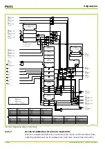
Страница 638: ...oseph Monier 92506 Rueil Malmaison FRANCE Phone 33 0 1 41 29 70 00 Fax 33 0 1 41 29 71 00 www schneider electric com Publication P631 EN M R 11 C Publishing Schneider Electric 07 2014 2014 Schneider E...

Отзывы: