www.procontechnology.com.au
8 Phone: (03) 98306288
Additional Output Ripple and Noise Control
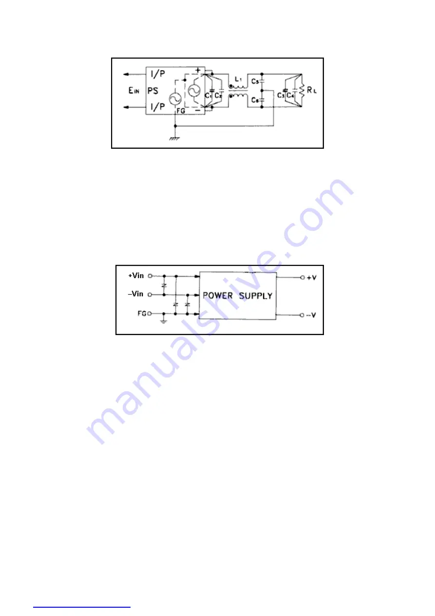
Fig. 17 is a diagram of a sample circuit that will improve the output ripple, noise, and Electromagnetic Interference (EMI) or
Common Mode Noise. Fig. 17 is an example circuit only. Further design considerations are essential for specific applications.
Fig. 17
Note: C1 & C3 are electrolytic capacitors and control the output ripple. Their values should be between 47uf and 100uf. C2, C4
& C5, C6 are high frequency ceramic capacitors and reduce the output noise. Their values range from 0.01uf and 0.1uf. The
value of inductance L1 is 0.5uH to 5uH.
Surge Voltage Control
Fig.18 shows a circuit used to control voltage surges that may be caused by power fluctuations or stray surges due to lightning.
The circuit has varistors connected bVin & –Vin, +Vin & FG, and –Vin & FG. This type of circuit is the minimum
recommended in areas where there are frequent lightning strikes.
Fig. 18


