MAX32600 User’s Guide
Pin Configurations, Packages, and Special Function Multiplexing
5
Pin Configurations, Packages, and Special Function Multiplexing
5.1
Pin Layout
There are two logical pin layouts available on the
MAX32600
which determine the location of certain multiplexed functions. The pin layout in effect is determined by
the state of an internal pad in the
MAX32600
package which can be bonded either to a high or low setting. The pin layout remapping is performed internal to the
MAX32600
and is independent of the actual pad-to-pin/ball packaging layout that occurs as part of the device assembly process.
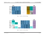
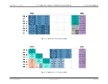
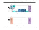
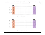
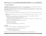
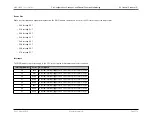
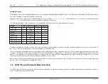
The two pin layouts are known as Standard and Compact, with pin functions available as follows (assuming all enabled pins are bonded out on the package used):
Standard Pin Layout
The Standard pin layout is featured on the 12mm x 12mm package and contains all GPIO ports available on the
MAX32600
(P0 through P7). It also includes LCD
functionality.
Compact Pin Layout
The Compact pin layout is featured on the 7mm x 7mm package and wafer-level packaging (WLP). It includes a reduced subset of the GPIO port pins, with only P0,
P1, and P2 available for use. The LCD function is not available on the Compact pin layout.
Note
On the WLP package, the package mux pin is brought out and must be strapped by the user circuit board.
Pin Function Mapping Between Layouts
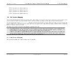
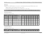
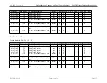
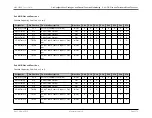
Certain GPIO-multiplexed pin functions are mapped differently depending on the enabled pin layout.
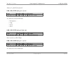
• P0[7:0] - Mapping is the same, except that current drive options are also included for the Compact layout.
• P1[3:0] - No differences.
• P1[7:4] - Different mapping on Standard vs. Compact layout.
• P2[3:0] - No differences.
• P2[7:4] - Different mapping on Standard vs. Compact layout.
• P3[7:0] - These pins exist on Standard layout only.
Rev.1.3 April 2015
Maxim Integrated
Page 165
Содержание MAX32600
Страница 1: ...MAX32600 User s Guide April 2015...

