- 2-21 -
Pin
Name
Input Function
CLK
System Clock
Active on the positive going edge to sample all inputs.
CS
Chip Select
Disables or enables device operation by masking or enabling all inputs except
CLK, CKE and L(U)DQM.
Masks system clock to freeze operation from the next clock cycle. CKE
CKE
Clock Enable
should be enabled at least one cycle prior to new command. Disable input
buffers for power down in standby.
A0~A10/AP
Address
Row/Column addresses are multiplexed on the same pins. Row address:
RA0~RA10, column address: CA0~CA7
BA
Bank Select Address
Selects bank to be activated during row address latch time. Selects bank for
read/write during column address latch time.
RAS
Row Address Strobe
Latches row addresses on the positive going edge of the CLK with RAS low.
Enables row access & precharge.
CAS
Column Address Strobe
Latches column addresses on the positive going edge of the CLK with CAS
low. Enables column access.
WE
Write Enable
Enables write operation and row precharge. Latches data in starting from
CAS, WE active.
L(U)DQM
Data Input / Output Mask
Makes data output Hi-Z, tSHZ after the clock and masks the output. Blocks
data input when L(U)DQM active.
DQ0~15
Data Input / Output
Data inputs/outputs are multiplexed on the same pins.
VDD/VSS
Power Supply/Ground
Power and ground for the input buffers and the core logic.
VDDQ/VSSQ
Data Output Power/Ground
Isolated power supply and ground for the output buffers to provide improved
noise immunity.
N.C/RFU
No Connection/
This is recommended to be left No Connection on the
Reserved for Future Use
device.
■
PIN Function table
■
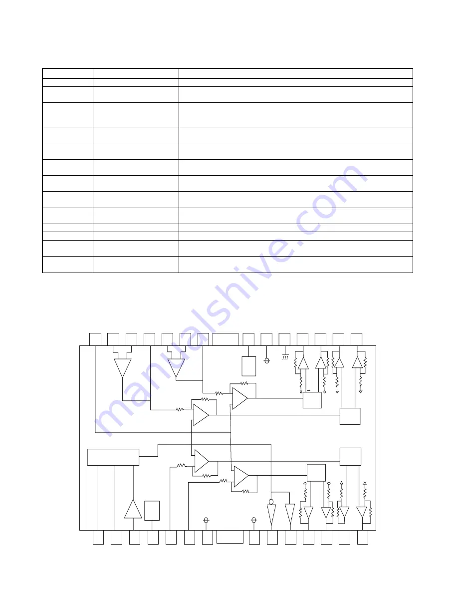
IC504 BA5810FM
28
27
26
25
24
23
22
21
20
19
18
17
16
15
1
2
3
4
5
6
7
8
9
10
11
12
13
14
+
+
—
+
—
+
—
+
—
+
—
7.5k
7.5k
7.5k
7.5k
LOADING PRE
FWE REV
X3
POWER
SAVE
16k
16k
16k
16k
PREVCC
(PRE. LODING)
PREVCC12
(CH1. CH2)
CD1~
CB4
MUTE
POWVCC34
(CH3, CH4)
10k
10k
10k
10k
10k
10k
10k
10k
LEVEL
SHIFT
LEVEL
SHIFT
LEVEL
SHIFT
LEVEL
SHIFT
10k
10k
10k
10k
10k
10k
Содержание TCH-M900
Страница 7: ... 2 3 ...
Страница 8: ... 2 4 ...
Страница 9: ... 2 5 ...
Страница 10: ... 2 6 ...
Страница 11: ... 2 7 ...
Страница 12: ... 2 8 ...
Страница 13: ... 2 9 ...
Страница 14: ... 2 10 ...
Страница 17: ... 2 13 IC401 LC875465B 1 PORT ASSIGNMENT INTERNAL BLOCK DIAGRAM of ICs ...
Страница 18: ... 2 14 2 PORT DESCRIPTION ...
Страница 21: ... 2 17 2 Block Diagram ...
Страница 26: ... 2 22 IC505 AMC1117 BLOCK DIAGRAM ...
Страница 30: ... SCHEMATIC DIAGRAM MAIN SCHEMATIC DIAGRAM 2 27 2 28 ...
Страница 31: ...2 29 2 30 FRONT SCHEMATIC DIAGRAM ...
Страница 32: ...2 31 2 32 SCHEMATIC DIAGRAM CDP SCHEMATIC DIAGRAM ...
Страница 34: ...2 35 2 36 3 MAIN P C BOARD ...
Страница 35: ...2 37 2 38 4 CDP P C BOARD ...


