ECP5 and ECP5-5G High-Speed I/O Interface
Technical Note
© 2014-2020 Lattice Semiconductor Corp. All Lattice trademarks, registered trademarks, patents, and disclaimers are as listed at
All other brand or product names are trademarks or registered trademarks of their respective holders. The specifications and information herein are subject to change without notice.
18
FPGA-TN-02035-1.3
ALIGNWD
Datain
Clkin
A
DELAYG
Z
ECLKI
STOP
ECLKO
SCLK
D
Q [3 :0 ]
RST
ALIGNWD
ECLK
IDDRX2F
Edge
Primary
Sclk
CLKDIVF
CLKI
RST
CDIVX
AlignWD
Q [3 : 0 ]
ECLKSYNCB
DEL_MODE=
ECLK_CENTERED
sync_reset
GDDR _SYNC
Sync
_ clk
Start
RST
START
SYNC _CLK
DDR _RESET
STOP
READY
Ready
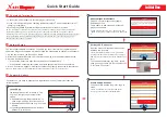
Figure 5.5. GDDRX2_RX.ECLK.Centered Interface (Static Delay)
Data _LoadN
Data _Move
Data _Direction
A
DELAYF
LOADN
MOVE
DIRECTION
CFLAG
Datain
Data _CFlag
Z
ECLKI
STOP
ECLKO
SCLK
D
RST
ALIGNWD
ECLK
Edge
Primary
Sclk
CLKDIVF
CLKI
RST
ALIGNWD
CDIVX
AlignWD
Clkin
Q [3:0]
Q [3:0]
IDDRX2F
ECLKSYNCB
sync_reset
GDDR _SYNC
Sync _clk
Start
RST
START
SYNC_CLK
DDR _RESET
STOP
READY
Ready
DEL_MODE=ECLK_CENTERED
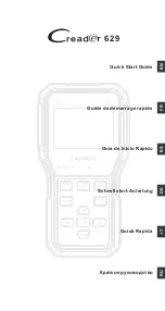
Figure 5.6. GDDRX2_RX.ECLK.Centered Interface (Dynamic Data Delay)
Interface Requirements
The clock input must use a PCLK input so that it can be routed directly to the Edge Clock tree.
ECLK must use the Edge Clock tree and the SCLK out of the CLKDIVF must use the Primary Clock tree, software
errors out if these dedicated clock routes are not used.
USE PRIMARY preference may be assigned to the SCLK net.
You must set the timing preferences as indicated in the
Timing Analysis for High Speed DDR Interfaces
section.
5.4.
GDDRX2_RX.ECLK.Aligned
Generic Receive DDR with the 2x gearing with ECLK. Input Clock is coming in edge aligned to the data. This interface
must be used for speeds above 400 MHz.
This DDR interface uses the following modules:
IDDRX2F element for 2x mode to capture the data
DDRDLLA/DLLDELD blocks are used to phase shift the incoming clock routed to the Edge Clock (ECLK) clock tree
through the ECLKSYNCB module.
CLKDIVF module is used to divide the incoming clock by 2.
Static data delay element DELAYG to delay the incoming data enough to remove the clock injection time
Optionally, you can choose to use Dynamic Data Delay adjustment using DELAYF element to control the delay on
the DATA dynamically. DELAYF also allows you to override the input delay set. The type of delay required can be
selected through Clarity Designer.
DEL_MODE attribute is used with DELAYG and DELAYF element to indicate the interface type so that the correct
delay value can be set in the delay element.
The ECLKBRIDGE can be optionally enabled if the data bus is crossing over between the left and right sides of the
device. If ECLKBRIDGE is enabled, then the ECLKBRIDGECS element should be used in the interface before the
ECLKSYNCB element. This element can be enabled through Clarity Designer.