


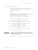


Keysight W6600A-series LPDDR4 BGA Interposers Installation Guide
49
Setting up the W6602A Interposer
6
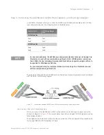
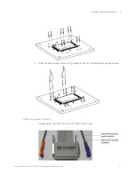
Step 1 - Soldering the W6602A Interposer
The W6602A interposer needs to be attached to the JEDEC LPDDR4 BGA 200 footprint on the
design to be probed. The desired DRAM is soldered to the top side of the interposer.
The recommended soldering sequence is:
• Riser
• Interposer
• DRAM
The interposer is designed to tolerate lead-free soldering temperature profiles. However, it is always
recommended to apply the minimum temperature required and the minimum number of
heating/cooling cycles to reduce risk of any damage to the interposer.
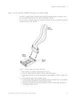
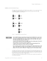
The stack up of these soldered components is illustrated in the following figure.
Figure 14
PC board, riser, interposer, and DRAM stack up
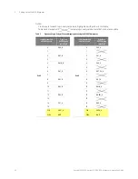
“W6600A-Series Interposers and Riser Soldering Guidelines"
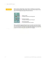
NOTE
A maximum of 10 mm wide X 15 mm long LPDDR4 DRAM package can fit on top of the
W6602A interposer without an additional riser or a socket between the DRAM and interposer
to provide clearance for the RC components.
Содержание LPDDR4
Страница 1: ...Keysight W6600A Series LPDDR4 BGA Interposers Installation Guide ...
Страница 4: ...4 Keysight W6600A series LPDDR4 BGA Interposers Installation Guide ...
Страница 8: ...8 Keysight W6600A series LPDDR4 BGA Interposers Installation Guide Contents ...
Страница 10: ...1 Introduction 10 Keysight W6600A series LPDDR4 BGA Interposers Installation Guide ...
Страница 78: ...Index 78 Keysight W6600A series LPDDR4 BGA Interposers Installation Guide ...
Страница 79: ...Keysight W6600A series LPDDR4 BGA Interposers Installation Guide 79 ...


