TKR-850
14
4. PLL Frequency Synthesizer
The PLL frequency synthesizer circuit consists of the fol-
lowing circuits : 4-1 receiver PLL circuit, 4-2 transmitter PLL
circuit, and 4-3 unlocked detector circuit.
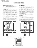
4-1. Receiver PLL
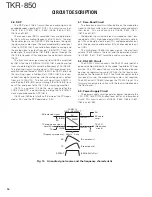
The receiver PLL circuit is located in VCO unit A3 (X58-
480) on TX-RX unit (X57-696 A/2), and consists of VCXO X2,
VCO’s (Q350 and Q351), a single-chip PLL IC IC300, buffer
amplifier Q355, and high-frequency amplifier Q302.
The VCXO generates 16.8MHz. The frequency stability is
within
±
1.5ppm (Temperature range of –30 to +60
°
C). The
frequency tuning of the VCXO is done to apply a voltage to
pin 1 of the VCXO. The output of the VCXO is applied to pin 8
of the PLL IC through the pin 7 of the VCO.
The first local oscillator is a lower heterodyne local oscilla-
tor, and the VCO oscillator frequency is 405.15 to 435.15MHz
(K), 395.15 to 425.15MHz (E), 435.15 to 467.15MHz (K2) or
355.15 to 385.15MHz (K3).
The oscillator frequency is controlled by applying the VCO
control voltage, obtained from the phase comparator to the
varactor diodes.
4-2. Transmitter PLL
The transmitter PLL circuit is located in VCO unit A2 (X58-
481) on TX-RX unit (X57-696 A/2), and consists of VCXO X3,
VCO’s (Q350 : K,K2,E, Q351 : K3), a single-chip PLL IC IC300,
buffer amplifier Q355, and high-frequency amplifier Q302.
The VCXO generates 16.8MHz. The frequency stability is
within
±
1.5ppm (Temperature range of –30 to +60
°
C). The
frequency tuning and modulation of the VCXO are done to
apply a voltage to pin 1 of the VCXO. The output of the VCXO
is applied to pin 8 of the PLL IC through the pin 7 of the VCO.
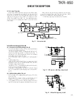
The VCO oscillator frequency is 450.00 to 480.00MHz (K),
440.00 to 470.00MHz (E), 480.00 to 512.00MHz (K2) or
400.00 to 430.00MHz (K3).
The oscillator frequency is controlled by applying the VCO
control voltage, obtained from the phase comparator to the
varactor diodes.
4-3. Unlock Detector Circuit
If a pulse signal appears at the LD pin of IC300, an unlock
condition occurs, causing the voltage applied to the pin of the
microprocessor to go low. The names of this pin are LDT for
TX PLL and LDR for RX PLL. When the microprocessor de-
tects this condition, the transmitter is disabled.
Q351
VCO unit (X58-480)
SRR
VCO A
IC300
VCO B
Q355
Q350
Q354
Q352
Q353
Q300
Q302
VCXO
X2
TX-RX unit
IC604
SW
SW
SW
AMP
AMP
LPF
PLL-IC
µ
-com
CP,DP
EPR,LDR
VCO unit (X58-481)
VCO A
IC300
Q355
Q350 : K,K2,E
Q300
Q302
VCXO
X3
TX-RX unit
IC604
AMP
AMP
LPF
PLL-IC
µ
-com
CP,DP
EPT,LDT
MO
VCO B
Q351 : K3
MO
MO
MO
Fig. 5
Receiver PLL
Fig. 6
Transmitter PLL
VCO A : 450~480 (K)
480~512 (K2)
440~470 (E)
VCO A : 440~460 (K,E)
480~500 (K2)
400~420 (K3)
VCO B : 460~480 (K,E)
500~512 (K2)
420~430 (K3)
Top view
TX VCO
(X58-481)
VCO B : 400~430 (K3)
RX VCO
(X58-480)
(MHz)
–44.850
–44.850
Fig. 7
VCO oscillation frequency
CIRCUIT DESCRIPTION

