background image


KPCMCIA-12AIAOH User’s Manual

I/O Registers

C-7


Example 1


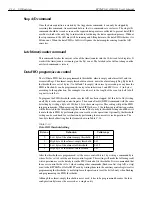
Refer to Table C-7. The following entries to the queue specify a scan list of three single-ended 
internal channels: 0, 12, and 7. Channel 0 has a gain of 10, and channels 12 and 7 have a gain 
of 100.


Example 2


Refer to Table C-8. The following entries to the queue specify a scan list of four differential inter-
nal channels: 2, 1, 6, and 7. Each channel has a gain of 1.


Channel configuration


Bits 4 and 5 (LSB) in a queue entry specify the gain on the external expansion card for the external 
channel selected by bits 3 through 0 of the same byte. Each expansion card has up to 16 channels 
(0, 1, 2, ... 15). Each channel may have up to four gain options: 1, 2, 4, or 8 if it is a low gain 
expansion card. 1, 10, 100, or 1000 if it is a high gain expansion card.

If there is no expansion card for the specified internal channel, the external channel and gain 
selection in the LSB will be ignored. However, the first channel mark on bit 7 should always be 
set properly.

The internal channel is selected by bits 8 through 11 (MSB), while the internal gain for the 
selected channel is specified by bits 12 and 13 (MSB). The internal gain can only be 1, 10, 100, 
or 1000.

Bit 14 (MSB) determines whether the input is differential (1) or single-ended (0). There are 16 
singled-ended channels but only eight differential channels. This bit should always be set to 0 if 
the selected internal channel is connected to an expansion card because the output from the 
expansion cards is always single-ended.

Bit 15 (MSB) is not used by the KPCMCIA-12AIAOH PC card. It should be set to 0.


Table C-7


Scan list queue programming example 1


Entry

Binary

Hex

Explanation


1

0001 0000 1000 0000

0180

Select channel 0, gain 10, first entry

2

0010 1100 0000 0000

2C00

Select channel 12, gain 100

3

0010 0111 0000 0000

2700

Select channel 7, gain 100


Table C-8


Scan list queue programming example 2


Entry

Binary

Hex

Explanation


1

0100 0010 1000 0000

4280

Select channel 2, gain 1, first entry

2

0100 0001 0000 0000

4100

Select channel 1, gain 1

3

0100 0110 0000 0000

4600

Select channel 6, gain 1

4

0100 0111 0000 0000

4700

Select channel 7, gain 1

Содержание KPCMCIA-12AIAOH

Страница 1: ...KPCMCIA 12AIAOH Type II PCMCIA Card User s Manual A G R E A T E R M E A S U R E O F C O N F I D E N C E...

Страница 2: ...ss such nonconformity in the Keithley Software Failure to notify Keithley of a nonconformity during the warranty shall relieve Keithley of its obligations and liabilities under this warranty Other Sof...

Страница 3: ...KPCMCIA 12AIAOH Type II PCMCIA Card User s Manual 1999 Keithley Instruments Inc All rights reserved Cleveland Ohio U S A Second Printing July 2002 Document Number 98936 Rev B...

Страница 4: ...into the manual Addenda are num bered sequentially When a new Revision is created all Addenda associated with the previous Revision of the manual are incorporated into the new Revision of the manual E...

Страница 5: ...s that a shock hazard exists when voltage levels greater than 30V RMS 42 4V peak or 60VDC are present A good safety practice is to expect that hazardous voltage is present in any unknown circuit befor...

Страница 6: ...components in mains circuits including the power transformer test leads and input jacks must be purchased from Keithley Instru ments Standard fuses with applicable national safety approvals may be use...

Страница 7: ...of Operation Introduction 3 2 DC DC power supply 3 2 Analog input multiplexer 3 3 Programmable gain control 3 3 Scan list 3 3 Trigger circuit 3 4 A D converter and data FIFO 3 4 Interrupt and status 3...

Страница 8: ...read only C 10 Digital output register base 3 write only C 11 Digital input register base 3 read only C 11 Pacer clock base 4 5 6 write only C 12 Command register base 7 write only C 12 Trigger arm co...

Страница 9: ...eory of Operation Figure 3 1 State transition diagram of A D conversion process 3 6 4 I O Connections Figure 4 1 KPCMCIA 12AIAOH PC card D 37 output connector KCAB AIAO 4 3 C I O Registers Figure C 1...

Страница 10: ...list queue entry bit definitions C 6 Table C 7 Scan list queue programming example 1 C 7 Table C 8 Scan list queue programming example 2 C 7 Table C 9 Control register bit definitions C 8 Table C 10 S...

Страница 11: ...1 Introduction...

Страница 12: ...rigger and pre trigger are two new features added to the KPCMCIA 12AIAOH PC cards One of the D A channels channel 1 can be used to set up the analog trigger level anywhere in the full input range of t...

Страница 13: ...te sampling rates from 0 006Hz to 100kHz 0 to 100kHz with external clock source Software TTL or analog trigger with programmable threshold Pre trigger capability up to the size of the data FIFO Two 12...

Страница 14: ...nt for repair include the following information Your name address and telephone number The invoice or order number and date of equipment purchase A description of the problem or its symptoms The RMA n...

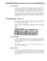
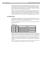
Страница 15: ...2 Installation...

Страница 16: ...the adapter into any type II PCMCIA socket All other configuration options are determined by the DriverLINX software and operating system as discussed in your DriverLINX documentation Software setup...

Страница 17: ...3 Theory of Operation...

Страница 18: ...eatures are programmable Functionally the KPCMCIA 12AIAOH PC card consists of the following components DC DC power supply Analog input multiplexer Programmable gain control A D converter Data FIFO Sca...

Страница 19: ...list entry via software The settling time of the analog front end meets the speed requirement However if the amplifier is saturated it may need a longer time to recover which may cause distortion in t...

Страница 20: ...clock fires and the scan results are placed in the data FIFO However once the almost full threshold programmed as an integer multiple of the scan list length of the data FIFO is reached the least rece...

Страница 21: ...e 3 write only of four output bits bits 0 to 3 The output port is latched but the input port is not Four input lines are connected to the digital input port each represents one bit in the port When re...

Страница 22: ...ine moves from S1 to S4 which can be set to 10 s 20 s or 40 s If there are more channels to scan in the list the state machine will skip to S1 for another conversion loop Other wise it will return to...

Страница 23: ...s In mode 1 the event is the timer overflow In mode 2 it is the external gate control going from low to high In mode 3 the event comes from the pacer clock In the synchronous update modes the data wor...

Страница 24: ...lue written into the reload register denoted as X for the sake of the discussion determines the divisor or modulus for timing and counting Since the final count before reloading is always 65535 hexade...

Страница 25: ...4 I O Connections...

Страница 26: ...tput 22 27 DA1 D A channel 1 output 20 7 GND Power supply ground return 19 24 ExtClk shared with A D Timer Counter external clock input 18 8 ExtGate Timer Counter external gate control 17 11 ExtOut Ti...

Страница 27: ...7 pin D shell connector If the cable is not identified as such do not use it with the KPCMCIA 12AIAOH PC cards Figure 4 1 KPCMCIA 12AIAOH PC card D 37 output connector KCAB AIAO 1 2 3 4 5 6 7 8 9 10 1...

Страница 28: ...5 Optional Accessories...

Страница 29: ...5 2 Optional Accessories KPCMCIA 12AIAOH User s Manual The following optional accessories are available from Keithley STP 37 STA U EXP 1600...

Страница 30: ...A Specifications...

Страница 31: ...eshold set in full A D input range 10V Rising falling directions 10mV hysteresis Sampling rate 0 006Hz to 100kHz with internal clock source External clock rate DC 5MHz NOTE In Paced mode the same inpu...

Страница 32: ...ower consumption 210mA full power 70mA power down Operating temperature 0 to 50 C Storage temperature 0 to 70 C Humidity 0 to 95 non condensing Size cable not included Standard PCMCIA type II Weight 1...

Страница 33: ...B PCMCIA Interface...

Страница 34: ...hat is routable to any system interrupt via the PCMCIA socket controller Two sets of registers are on the KPCMCIA 12AIAOH PC card the configuration registers and program registers The configuration re...

Страница 35: ...rd I O card Card configuration and status register CCSR Refer to Table B 3 The KPCMCIA 12AIAOH PC card uses two bits in this register When bit 1 is set to 1 it indicates a pending interrupt The bit wi...

Страница 36: ...C I O Registers...

Страница 37: ...rs can be accessed as 16 bit I O registers They can also be accessed with 8 bit I O instructions The remaining registers are 8 bit wide Each entry in Table C 1 is discussed in detail in the following...

Страница 38: ...ation the 16 bit word read from or written into the register has different meanings as described in Table C 3 The selection bit in Table C 3 is also called the program access control bit as defined in...

Страница 39: ...written into the FIFO will be returned The data FIFO reg ister is read only under this mode You cannot write data bytes into the data FIFO through I O instructions Mode setting The FIFO operation mode...

Страница 40: ...e data FIFO register provided no more data bytes are written into the FIFO by the A D converter under mode 1 or 3 The same happens to the FIFO almost full flag if the data bytes available in the FIFO...

Страница 41: ...aranteed The scan list queue is write only The scan list queue should be flushed before writing any entries into it Refer to Command reg ister base 7 write only for information about the scan list que...

Страница 42: ...7 should always be set properly The internal channel is selected by bits 8 through 11 MSB while the internal gain for the selected channel is specified by bits 12 and 13 MSB The internal gain can onl...

Страница 43: ...ng also indicates that all digital output lines bits 0 to 3 will be used for external channel selection and two of the four digital input lines bits 1 and 3 will be used for external gain selection A...

Страница 44: ...r signal is chosen as the trigger edge if the bit is set to 1 Otherwise the rising edge is selected The edge selection will be ignored if the internal trigger source is specified For the analog trigge...

Страница 45: ...flag It is 0 when the PC card is in the process of scan ning the input channels specified by the scan list and 1 when it is finished Bit 6 is the A D running flag A 1 here indicates that the A D is bu...

Страница 46: ...egister base 3 read only As mentioned before two of the digital input lines are shared with external trigger bit 0 and external clock bit 2 The other two lines are also used for external gain control...

Страница 47: ...counter is reloaded The pacer clock generation continues until the KPCMCIA 12AIAOH PC card receives the stop command represented by writing a 1 at bit 4 of the command register Refer to Com mand regis...

Страница 48: ...up The flush command may also be followed by FIFO threshold programming After the FIFO is flushed the FIFO empty flag is set to 1 and the almost full and full flag reset to 0 The flush FIFO command al...

Страница 49: ...his bit to 0 by writing an all 0 byte to the auxiliary control register Then send a flushA D FIFO command with the same bit setting by writing a byte of 40H hex 40 to the same register This setting wi...

Страница 50: ...o 15 select the D A channel in which bits 13 14 and 15 must all be set to 0 and bit 12 is either set at 0 to select D A channel 0 or 1 to select D A channel 1 Refer to Table C 15 for bit definitions D...

Страница 51: ...ay either be passed immediately into the output register direct update mode or loaded into the output register upon receiving the synchronous event synchronous update modes Bits 1 and 0 of the auxilia...

Страница 52: ...Bits 3 and 4 in the auxiliary control register base 15 write determine the timer modes as sum marized in Table C 17 Mode 0 is used to reload the up counter Note that the reloading only takes place wh...

Страница 53: ...s 65535 or hexadecimal FFFF Suppose D is the divisor also called modulus for counter of the timer and X is the value written into the reload register The relation between the two is D 65536 X The up c...

Страница 54: ...mer counter port base 10 base 11 in this section for more information Bits 1 and 0 specify the D A update modes Refer to Section 3 and D A update modes in this section for more information Table C 18...

Страница 55: ...by writing a 0 into bit 5 of the auxiliary control register Refer to Section 3 and Timer counter port base 10 base 11 in this section for more information Bit 5 tells whether the D A port buffer regis...

Страница 56: ...CCSR B 3 Channel configuration C 7 Clock source C 8 Command register base 7 write only C 12 Configuration and option register COR B 3 Control register base 2 write only C 8 D D A channel output C 15 D...

Страница 57: ...control 3 3 R Reading the contents of the timer counter C 18 S Scan list 3 3 Scan list queue programming C 6 Scan list queue register base 1 write only C 6 Scan rate selection C 15 Software setup 2 2...

Страница 58: ...e 65 82110 Germering 089 84 93 07 40 Fax 089 84 93 07 34 GREAT BRITAIN Unit 2 Commerce Park Brunel Road Theale Berkshire RG7 4AB 0118 929 7500 Fax 0118 929 7519 INDIA Flat 2B Willocrissa 14 Rest House...

Отзывы: