


JOHNSON CONTROLS
231
FORM 201.23-NM2
ISSUE DATE: 3/9/2015
8
VSD OPERATION AND CONTROLS
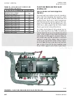
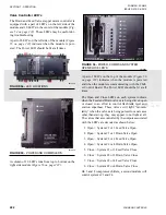
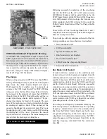
VSD Logic Board
The VSD Logic Board communications with the Chill-
er Control Board via comms and controls the VSD
functions. It converts the frequency and run commands
from the Chiller Control Board into the necessary volt-
age and frequency commands to operate the inverter
section. It also controls the converter section of the
drive (AC Line to DC Bus conversion) by controlling
the pre-charge function.
The VSD Logic Board contains a 2nd microprocessor
(motor controller) that generates the PWM signals that
control the IGBT outputs in the inverter section of the
VSD.
An FPGA handles the hardware safeties that can shut
down the VSD much faster than the software safeties.
The VSD Logic Board handles all of the VSD related
safeties, which includes motor current, BUS voltage,
and other safeties.
The VSD Logic Board reports shutdown information
back to the Chiller Control Board via the RS-485 com-
munication link.
2, 3 and 4 compressor chillers all use the same soft-
ware. The microprocessor determines whether the
chiller is a 2, 3 or 4 compressor chiller by electroni-
cally checking for a factory-installed jumper in the sys-
tem wiring harness. The microprocessor checks for the
jumper located in the J1 plug wiring harness at power-
up. If no jumper or more than one jumper is sensed, the
microprocessor will inhibit start-up. Details regarding
the location of the jumper are provided in
figuration Jumpers on page 207
VSD Start/run Initiation
Following a successful precharge of the DC Bus and
a run command from the Chiller Control Board, the
VSD Logic Board microprocessor will determine the
motor output voltage (% modulation) and the output
frequency required based on the operating frequency
command from the Chiller Control Board. This infor-
mation will then be sent to the PWM generator located
on the VSD Logic Board.
On start-up, the output frequency from the VSD to the
motor(s) will be increased from 0 Hz to the operating
frequency commanded by the Chiller Control Board.
The rate of change of the frequency will also be con-
trolled by the VSD Logic Board.
The rate of change of the output frequency at start-up,
during acceleration is 10 Hz/sec between 0 and 50 Hz
and 30.4 Hz/sec above 50 hertz. The maximum rate
of change of the output frequency during deceleration
between 200 and 100 Hz is 30.4 Hz/sec, and 100 and 0
Hz is 10 Hz/sec.
The VSD Logic Board and its PWM generator will re-
ceive operating frequency and voltage commands from
the Chiller Control Board based on the load.
When a frequency (speed) change is requested from
the Chiller Control Board, the chiller microprocessor
will send the change to the VSD Logic Board and the
VSD Logic Board will acknowledge it accepted the
change. Loading and unloading will take place at the
rate of 0.1 to 1Hz every 2 seconds.
PWM Generator Type and Carrier Frequency
The PWM generator is responsible for providing asym-
metrical uniform sampled PWM waveforms to the
compressor motor at a carrier frequency of 3125 Hz by
turning on an off the inverter IGBT’s. The waveform
generated is equivalent to a specific V/F ratio at a given
speed based on the voltage and frequency commands
from the Chiller Control Board. The PWM Generator
receives operating frequency and voltage commands
from the VSD Logic Board control processor.
Short Circuit Protection Minimum Output
Pulse Width and Interlock Delay
The PWM generator is programmed to drop all “on”
pulses in less than 10 microseconds (and all matching
“off” pulses in the mirrored waveform) to permit time
for the IGBT gate drivers to detect and self extinguish
an inverter short circuit condition.
Modulating Frequency
The modulating frequency range will range from 0 to
200 Hz. The modulating frequency waveform con-
sists of a sinusoidal waveform summed together with
16.66% of the third harmonic component of the sinu-
soidal waveform. Utilization of this waveform as the
modulating waveform will permit the drive to generate
a fundamental line to line voltage equal to the DC Bus
voltage divided by 1.414.
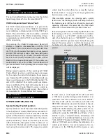
SECTION 8 - MICROPANEL
Содержание YCIV0157
Страница 18: ...JOHNSON CONTROLS 18 FORM 201 23 NM2 ISSUE DATE 3 9 2015 SAFETY SYMBOLS THIS PAGE INTENTIONALLY LEFT BLANK ...
Страница 38: ...JOHNSON CONTROLS 38 FORM 201 23 NM2 ISSUE DATE 3 9 2015 THIS PAGE INTENTIONALLY LEFT BLANK ...
Страница 42: ...JOHNSON CONTROLS 42 FORM 201 23 NM2 ISSUE DATE 3 9 2015 THIS PAGE INTENTIONALLY LEFT BLANK ...
Страница 50: ...JOHNSON CONTROLS 50 FORM 201 23 NM2 ISSUE DATE 3 9 2015 THIS PAGE INTENTIONALLY LEFT BLANK ...
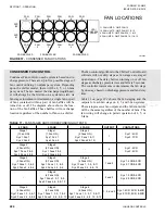
Страница 104: ...JOHNSON CONTROLS 104 FORM 201 23 NM2 ISSUE DATE 3 9 2015 SECTION 6 TECHNICAL DATA Panel Layout 2 Compressor Models ...
Страница 105: ...JOHNSON CONTROLS 105 SECTION 6 TECHNICAL DATA FORM 201 23 NM2 ISSUE DATE 3 9 2015 THIS PAGE INTENTIONALLY LEFT BLANK ...
Страница 115: ...JOHNSON CONTROLS 115 SECTION 6 TECHNICAL DATA FORM 201 23 NM2 ISSUE DATE 3 9 2015 THIS PAGE INTENTIONALLY LEFT BLANK ...
Страница 119: ...JOHNSON CONTROLS 119 SECTION 6 TECHNICAL DATA FORM 201 23 NM2 ISSUE DATE 3 9 2015 THIS PAGE INTENTIONALLY LEFT BLANK ...
Страница 333: ...JOHNSON CONTROLS 333 FORM 201 23 NM2 ISSUE DATE 3 9 2015 NOTES ...


