background image

EMI and Mechanical Design Considerations

152

Design Guide

Differential clocking can also reduce the amount of noise coupled to other traces, which improves 
signal quality and reduces EMI. I/O signals are particularly important because they often leave the 
system chassis (serial and parallel ports, keyboards, mouse, etc.), and radiate noise that has been 
induced onto them. A single-ended clock's return path is usually a reference plane, which is shared 
by other signals/traces. When noise is created on a single-ended clock, the noise will appear on the 
reference plane and may be coupled to I/O traces. A differential clock's return path is the clock-bar 
signal/trace, which is more isolated than the reference plane and minimizes potential I/O trace 
coupling.

For best results, the trace lengths and routing of the clock lines must be closely matched, and 
spacing between the two traces should be kept as small as possible. This will minimize loop area 
and maximize H-field cancellation. In addition, the real and parasitic terminations of each signal of 
a differential pair should be the same. Also, the skew between the signal level transitions on the 
two lines must be small compared to the rise time of the level transitions.

Placing ground traces on the outside of the differential pair may further reduce emissions. 
Intermediate vias to ground may be needed to reduce the opportunity for re-radiation from the 
ground traces themselves. Distance between vias should be less than ¼ of a wavelength of the fifth 
harmonic of the processor core frequency.

11.2.3

PCI Bus Clock Control

Experimental data has indicated a reduction in EMI may be possible by disabling the clocks to 
unused (and therefore unterminated) PCI slots. CK408B, the clock chip that has been specified and 
designed for this platform, supports individual control of the various PCI clocks. Designers have 
the option to enable or disable individual PCI clocks depending upon their specific system 
configuration requirements. Refer to the 

CK408B Clock Synthesizer Design Guidelines

 for details 

on how to configure the PCI clocks.

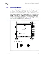
Figure 11-3. Cancellation of H-fields Through Inverse Currents

CLK - clock trace

CLK' - clock bar

trace

H-field

caused by

Iclk

Iclk

Iclk'

H-field

caused by

Iclk'

Содержание Xeon

Страница 1: ...Intel Xeon Processor with 512 KB L2 Cache and Intel E7500 Chipset Platform Design Guide March 2002 Document Number 298649 002 ...

Страница 2: ...em The Intel E7500 chipset and processors in the Intel Xeon processor family may contain design defects or errors known as errata which may cause the product to deviate from published specifications Current characterized errata are available on request Contact your local Intel sales office or your distributor to obtain the latest specifications and before placing your product order I2C is a two wi...

Страница 3: ...acement 31 3 2 Platform Stack Up 32 4 Platform Clock Routing Guidelines 35 4 1 Clock Groups 38 4 1 1 HOST_CLK Clock Group 38 4 1 1 1 HOST_CLK Clock Topology 38 4 1 1 2 HOST_CLK General Routing Guidelines 41 4 1 1 3 CK408 vs CK408B Requirement 41 4 1 2 CLK66 Clock Group 42 4 1 2 1 CLK66 Skew Requirements 43 4 1 3 CLK33_ICH3 S Clock 45 4 1 4 CLK33 Clock Group 46 4 1 5 CLK14 Clock Group 48 4 1 6 USBC...

Страница 4: ... 7 2 Hub Interface 2 0 Implementation 84 7 2 1 Hub Interface 2 0 High Speed Routing Guidelines 84 7 2 2 Hub Interface 2 0 Generation Distribution of Reference Voltages 87 7 2 3 Hub Interface 2 0 Resistive Compensation 88 7 2 4 Hub Interface 2 0 Decoupling Guidelines 89 7 2 5 Unused Hub Interface 2 0 Interfaces 89 7 3 Hub Interface 1 5 Implementation 89 7 3 1 Hub Interface 1 5 High Speed Routing Gu...

Страница 5: ... 8 2 6 6 Pull Ups Pull Downs in Dual Slot Parallel Mode 108 8 2 6 7 Hot Plug Muxed Signals in Dual Slot Parallel Mode 109 8 2 6 8 SMBus Address Considerations 110 8 2 6 9 Reference Schematic for Dual Slot Parallel Mode 111 8 2 7 Three or More Slot Serial Mode 112 8 2 7 1 Hot Plug and Non Hot Plug Combinations 112 8 2 7 2 Required Additional Logic 112 8 2 7 3 Debounced Hot Plug Switch Input 112 8 2...

Страница 6: ...outing and Layout 136 9 7 1 3 Crosstalk Consideration 136 9 7 1 4 Impedances 136 9 7 1 5 Line Termination 136 9 7 2 General LAN Routing Guidelines and Considerations 137 9 7 2 1 General Trace Routing Considerations 137 9 7 2 2 Trace Geometry and Length 138 9 7 2 3 Signal Isolation 138 9 7 2 4 Power and Ground Connections 138 9 7 2 5 General Power and Ground Plane Consideration 139 9 7 2 6 Board De...

Страница 7: ...12 2 4 Voltage Regulator Requirements 164 12 2 4 1 Input Voltages and Currents 165 12 2 4 2 Power Good Output PWRGD 165 12 2 4 3 Fault Protection 166 12 2 5 VR Module 9 1 Recommendations 166 12 2 6 VR Down Recommendations 167 12 2 7 Voltage Sequencing 169 12 2 8 VCCA VCCIOPLL and VSSA Filter Specifications 171 12 2 9 Processor Decoupling 173 12 2 9 1 High Frequency Decoupling 173 12 2 9 2 Bulk Dec...

Страница 8: ...quencing Requirement 186 13 Schematic Checklist 187 13 1 Processor Schematic Checklist 187 13 2 MCH Schematic Checklist 193 13 3 Intel ICH3 S Schematic Checklist 196 13 4 Intel 82870P2 P64H2 Schematic Checklist 204 13 5 CK408 Schematic Checklist 209 14 Layout Checklist 211 14 1 Processor Checklist 211 14 2 Intel E7500 MCH Layout Checklist 213 14 3 Intel ICH3 S Layout Checklist 216 15 Schematics 22...

Страница 9: ...B_CLK 49 4 15 Decoupling Capacitors Placement and Connectivity 50 5 1 Dual Processor System Bus Topology 54 5 2 Trace Length Matching for the Dual Processor System Bus 57 5 3 RESET Topology 59 5 4 Topology for Asynchronous GTL Signals Driven by the Processor 60 5 5 Recommended THERMTRIP Circuit 61 5 6 Topology for Asynchronous GTL Signals Driven by the Chipset 61 5 7 Topology for PWRGOOD CPUPWRGOO...

Страница 10: ... 10 MUX Circuit Example 105 8 11 Single Slot Parallel SMBus Circuit 106 8 12 Reference Schematic for Single Slot Parallel Mode 107 8 13 Dual Slot Parallel SMBus Circuit 110 8 14 Reference Schematic for Dual Slot Parallel Mode 111 8 15 Four Slot Stutter Logic Implementation Example 113 8 16 Reference Schematic for Serial Mode 114 8 17 M66EN Isolation Switch Solution 116 8 18 M66EN Diode Solution 11...

Страница 11: ...12 5 Example Load Line Selection Circuit 168 12 6 VID Routing 169 12 7 Power Up and Power Down Timing 170 12 8 Processor Filter Topology 171 12 9 Filter Implementation 1 Using Discrete Resistor 172 12 10 Filter Implementation 2 No Discrete Resistor 172 12 11 Decoupling Example for a Microstrip Baseboard Design 174 12 12 1206 Capacitor Pad and Via Layouts 174 12 13 GTLREF Divider 175 12 14 Suggeste...

Страница 12: ...nchronous Signal Group Routing Guidelines 71 6 4 Command Clock Pair Routing Guidelines 73 6 5 Source Clocked Signal Group Routing Guidelines 75 6 6 Chip Select Routing Guidelines 76 6 7 Clock Enable Routing Guidelines 77 7 1 Hub Interface 2 0 Signal Strobe Association 84 7 2 Hub Interface 2 0 Signal Groups 84 7 3 Hub Interface 2 0 Routing Parameters 84 7 4 Hub Interface 2 0 Reference Circuit Speci...

Страница 13: ...lk Capacitance Recommendations 175 12 7 Various Component Models Used at Intel Not Vendor Specifications 177 12 8 ICH3 S Power Rail Terminology 183 12 9 Intel ICH3 S Decoupling Recommendations 184 12 10 Intel P64H2 Max Sustained Currents 185 12 11 Decoupling Capacitor Recommendations 185 13 1 Processor Schematic Checklist 187 13 2 MCH Schematic Checklist 193 13 3 Intel ICH3 S Schematic Checklist 1...

Страница 14: ...ision Description Date 001 Initial Release February 2002 002 Changed Section 6 3 DDR Command Clock Figure Notes Added Section 12 5 4 New P64H2 Power Sequencing Requirement Updated Schematics to reflect changes identified above March 2002 ...

Страница 15: ...n implementation the core schematics remain the same for most E7500 chipset based platforms The schematic set provides a reference schematic for each E7500 chipset component as well as common motherboard options Additional flexibility is possible through other permutations of these options and components 1 1 Reference Documentation Note For the latest revision and documentation number contact your...

Страница 16: ...or Voltage Regulator Down VRD Design Guidelines http developer intel com design Xeon guides Intel Xeon Processor with 512 KB L2 Cache System Compatibility Guidelines http developer intel com design Xeon guides Intel Xeon Processor Thermal Design Guidelines http developer intel com design Xeon guides 298348 htm Intel Xeon Processor Thermal Solution Functional Specifications http developer intel com...

Страница 17: ...e processor to recognize them Bus Agent A component or group of components that when combined represent a single load on the AGTL bus Core Power Core power refers to a power rail that is on only during full power operation These power rails are on when the active low PSON signal is asserted to the power supply The core power rails that are distributed directly from the power supply are 12 V 5 V an...

Страница 18: ...tion on the interconnect delay For example when a signal is transmitted down a line and the reflections due to the transition have not completely dissipated the following data transition launched onto the bus is affected ISI is dependent upon frequency time delay of the line and the reflection coefficient at the driver and receiver ISI can impact both timing and signal integrity Network The networ...

Страница 19: ...form refer to the component datasheets listed in Section 1 1 Simultaneous Switching Output SSO Effects which are differences in electrical timing parameters and degradation in signal quality caused by multiple signal outputs simultaneously switching voltage levels in the opposite direction from a single signal or in the same direction These are called odd mode and even mode switching respectively ...

Страница 20: ...t compatible with the Pentium III Xeon processor bus The system bus uses source synchronous transfer of address and data to improve performance and enables addressing at 2X the system bus frequency of 100 MHz and data transfers at 4X the system bus frequency of 100 MHz This allows the processors to transfer data at 3 2 GB s The Xeon processor provides manageability features consistent with Intel P...

Страница 21: ...t system bus addressing model 12 deep in order queue 2 deep defer queue Memory Bus Features 144 bit wide DDR 200 memory interface with memory bandwidth of 3 2 GB s Supports x72 ECC registered DDR 200 DIMMs using 64 Mb 128 Mb 256 Mb and 512 Mb DRAMs Supports a maximum of 16 GB of memory Supports Single 4 bit Error Correct Double 4 bit Error Detect S4EC D4ED Chipkill technology ECC x4 Chipkill techn...

Страница 22: ...ecification Revision 2 2 compliant interface PCI Local Bus Specification Revision 2 2 compliant interface Integrated LAN Controller 1 3 2 3 PCI PCI X 64 bit Hub 2 Intel 82870P2 P64H2 The P64H2 provides PCI PCI X high performance I O capability on E7500 chipset based platforms Each P64H2 component includes 16 bit HI2 0 Connection to MCH 1 GB s point to point connection for I O bridges with ECC prot...

Страница 23: ...ystem Bus Data 100 4 8 3200 DDR Interface 100 2 16 3200 Hub Interface A 66 4 1 266 Hub Interface B C D 66 8 2 1066 PCI X 133 1 8 1066 Figure 1 1 Example Intel Xeon Processor with 512 KB L2 Cache Intel E7500 Chipset Based System Configuration Intel ICH3 S MCH USB 1 1 6 Ports AC 97 Codec s AC 97 2 1 1 4 FWHs 10 100 LAN Controller 4 IDE Devices UltraATA 100 System Memory GPIOs Processor Processor SMB...

Страница 24: ...Introduction 24 Design Guide This page is intentionally left blank ...

Страница 25: ...rs should use only the exact ball assignment to conduct routing analyses Reference the following documents for exact ball assignment information Intel Xeon Processor with 512 KB L2 Cache at 1 80 GHz 2 GHz and 2 20 GHz Datasheet Intel 82801CA I O Controller Hub 3 ICH3 S Datasheet Intel PCI 64 Hub 2 P64H2 Datasheet Intel E7500 Chipset Memory Controller Hub MCH Datasheet ...

Страница 26: ...L2 Cache Quadrant Layout Top View Vcc Vss ADDRESS DATA Vcc Vss CLOCKS SMBus COMMON CLOCK COMMON CLOCK Async JTAG Signal Power Ground Reserved NC A C E G J L N R U W AA AC AE B D F H K M P T V Y AB AD 3 5 7 9 11 13 15 17 19 21 23 25 27 29 31 1 GTLREF SM_VCC A C E G J L N R U W AA AC AE B D F H K M P T V Y AB AD 2 4 6 8 10 12 14 16 18 20 22 24 26 28 ...

Страница 27: ... Bus HI_A D AM AN AL AK AJ AH AF AG AE AD AC AB Y AA W V U T P R N M L K H J G F E D C B A AM AN AL AK AJ AH AF AG AE AD AC AB Y AA W V U T P R N M L K H J G F E D C B A 33 32 31 30 29 28 27 26 25 24 23 22 21 20 19 18 17 16 15 14 13 12 11 10 9 8 7 6 5 4 3 2 1 33 32 31 30 29 28 27 26 25 24 23 22 21 20 19 18 17 16 15 14 13 12 11 10 9 8 7 6 5 4 3 2 1 ...

Страница 28: ... AC AB AA Y W V T R U P N M L K J H G F E D C B A AC AB AA Y W V T R U P N M L K J H G F E D C B A 22 21 20 19 18 17 16 14 13 12 11 10 9 8 7 6 5 4 3 2 1 15 O O O LAN AC 97 EEPROM VSS VCC_1 8 VCCSUS_1 8 CLK IDE HUB Interface NC VCC_3 3 USB GPIO VCCSUS_3 3 CPU RTC SMBus Misc VCC LPC Firm Ware LAN USB HUB Interface CPU IDE SMBus GPIO PCI 23 O O O O O O O O O O O O O O O O O O O O O LPC ...

Страница 29: ...6 14 13 12 11 10 9 8 7 6 5 4 3 2 1 AD AC AB AA Y W V T R U P N M L K J H G F E D C B A 24 22 23 21 20 19 18 17 16 15 14 13 12 11 10 9 8 7 6 5 4 3 2 1 AD AC AB AA Y W V T R U P N M L K J H G F E D C B A 15 VCC3 3 VSS PB VCC1 8 VCC5REF HP HI PBIRQ PSTRB PA APIC PAIRQ O MISC BPCLK SCLK SDATA PCI PCI X Channel A PCI PCI X Channel B IRQs Hub Interface Hot Plug ...

Страница 30: ...Component Quadrant Layout 30 Design Guide This page is intentionally left blank ...

Страница 31: ... cache Intel E7500 chipset based customer reference board E7500 CRB Table 3 1 lists the assumptions used for the component placement Refer to www ssiforum org for detailed information on the SSI Server System Infrastructure specification Table 3 1 Assumptions for System Placement Example System Configuration Assumptions Form Factor SSI Specification Number of PCB Layers Assembly DP Server Midrange...

Страница 32: ...only Route signals on layers 4 and 5 orthogonally to reduce crosstalk between the layers Intel strongly recommends that system designers use the stack up shown in Figure 3 2 and recommendations in Table 3 2 when designing their boards Intel realizes numerous ways exist to achieve these targeted impedance tolerances contact your board vendor for these specifics Intel encourages platform designers t...

Страница 33: ...via size is 0 014 mil finished in a 0 026 mil land with 0 040 mil antipad Approximately 15 000 plated through holes total Finish Solder Mask On Bare Copper SMOBC Soldermask Type SM 840 minimum web 0 004 mils Fabrication Edge Routed Component Technology Through hole SMT QFP BGA Front side Discrete 0603 0805 Back side Core 5 2 mil Dielectric 9 6 mil 2 1 mil 1 oz plating Power Dielectric Signal Signa...

Страница 34: ...Platform Stack Up and Component Placement Overview 34 Design Guide This page is intentionally left blank ...

Страница 35: ...five 66 MHz speed clocks that drive all I O buses Figure 4 1 shows the implementation of the bus clocks for this configuration For more information on CK408B compliance refer to the CK408B Clock Synthesizer Specification Specifically for E7500 Chipset DP with ITP System Clock Generator Document Table 4 1 CK408B Clock Groups Clock Group Name Frequency MHz Receiver Host_CLK 100 Processor 0 Processor...

Страница 36: ...rocessor 0 BCLK 0 CPU Processor 0 BCLK 1 CPU Processor 1 BCLK 0 CPU Processor 1 BCLK 1 CPU MCH HCLKINP CPU MCH HCLKINN CLK66 66BUF MCH 66IN ICH3 S CLK66 P64H2 CLK66 CLK33_ICH3 S PCIF ICH3 S PCICLK CLK14 REF0 ICH3 S CLK14 SIO CLOCKl CLK33 PCI PCI Connector 1 CLK PCI Connector 2 CLK PCI Connector 3 CLK PCI Connector 4 CLK PCI Connector 5 CLK FWH CLK SIO PCI_CLK PCIF BMC LCLK USBCLK USB 48MHZ ICH3 S ...

Страница 37: ... 33MHz CPU CPU 4 PCIF 3 PCI 7 66BUF 5 CLK33 x7 CLK33 x5 DIMMclk x4 pr DDR Channel A MCH ITP Processor Processor Intel ICH S CK408B Intel P64H2 P C I P C I P C I P C I P C I P C I P C I P C I PCIclk x7 P C I P C I P C I P C I P C I P C I P C I P C I P C I P C I P C I P C I P C I P C I P C I P C I Host_CLK DDR Channel B DIMMclk x4 pr PCIclk x7 PCIclk x7 PCIclk x7 PCIclk x7 PCIclk x7 USBCLK USB 48MHz...

Страница 38: ...ure load requirements The recommended termination for the differential bus clock is a Shunt Source Termination Refer to Figure 4 2 for an illustration of this termination scheme Parallel Rt resistors perform a dual function converting the current output of the clock driver to a voltage and matching the driver output impedance to the transmission line The series resistors Rs provide isolation from ...

Страница 39: ...Spacing Maintain a minimum S h ratio of 5 26 Keep parallel serpentine sections as short as possible Minimize 90 degree bends Make 45 degree bends if possible Figure 4 4 Motherboard Impedance Differential 100 Ω typical 8 Motherboard Impedance Single Ended 50 Ω 10 9 Processor Routing Length L1 L1 Clock Driver to Rs 0 0 5 Figure 4 2 13 Processor Routing Length L2 L2 Rs to Rs Rt Node 0 0 2 Figure 4 2 ...

Страница 40: ...pair should be targeted to be of equal value They should have the same physical construction If the HOST_CLK traces vary within the tolerances specified both traces of a differential pair must vary equally 10 Length compensation for the processor socket and package delay is added to chipset routing to match electrical lengths between the chipset and the processor from the die pad of each Therefore...

Страница 41: ...s CK408B Requirement The CK408 and CK408B are pin compatible The only difference between the two chips is the CK408B replaces two signals on the CK408 with a fourth HOST_CLK pair for the In_Target_Probe ITP and is preferred by board designers for preliminary testing and validation While the CK408B pins need to be connected to the ITP the CK408 pins require the following stuffing options Add one 10...

Страница 42: ...pology for CLK66 Table 4 4 CLK66 Routing Guidelines Parameters Routing Guidelines Clock Group CLK66 Topology Point to Point Reference Plane Ground referenced contiguous over entire length Characteristic Trace Impedance Z0 50 Ω 10 Trace Width 5 mils Trace Spacing 25 mils Trace Length L1 0 00 0 50 Trace Length L2 3 00 9 0 Resistor R1 43 Ω 5 Skew Requirements All the clocks in the CLK66 group must ha...

Страница 43: ...ng the components on a riser in which case the riser card trace length designator Y should also be accounted for as yet another factor In this case the last equation would become X 0 34 0 60 Z 0 60 Y X 1 54 Y Z refer to Figure 4 9 Note that if a riser is used the motherboard clock trace must be designed for the specific riser card trace length and connector NOTES 1 All lengths must be matched with...

Страница 44: ... from CK408B to MCH must be between 3 and 9 5 4 Each connector is equivalent to 0 60 of trace 5 Each riser is equivalent to 0 60 Y where Y is the riser card trace length 6 The riser must be built with the CLK66 trace length matched to the motherboard routed length Figure 4 8 Example of Adding a Single Connector Total Length X 43 Ω MCH Intel P64H2 43 Ω Z Motherboard Trace Length X 0 34 0 60 Z X 0 9...

Страница 45: ...gy for CLK33_ICH3 S Table 4 5 CLK33_ICH3 S Routing Guidelines Parameter Routing Guidelines Clock Group CLK33_ICH3 S Topology Point to Point Reference Plane Ground referenced contiguous over entire length Characteristic Trace Impedance Z0 50 Ω 10 Trace Width 5 mils Trace Spacing 25 mils Trace Length L1 0 00 0 50 Trace Length L2 3 00 9 0 Resistor R1 33 Ω 5 Skew Requirements Must be matched to 100 mi...

Страница 46: ...idelines for PCI Device Down Parameter Routing Guidelines Clock Group CLK33 Topology Point to Point Reference Plane Ground referenced contiguous over entire length Characteristic Trace Impedance Z0 50 Ω 10 Trace Width 5 mils Trace Spacing 25 mils Trace Length L1 0 00 0 50 Trace Length L2 3 00 9 0 Resistor R1 33 Ω 5 Skew Requirements PCI device PCI device skew max allowed by PCI Local Bus Specifica...

Страница 47: ...aracteristic Trace Impedance Z0 50 Ω 10 Trace Width 5 mils Trace Spacing 10 mils Trace Length L1 0 00 0 50 Trace Length L2 3 00 9 0 Trace Length C Routed 2 50 per PCI Local Bus Specification Rev 2 2 Resistor R1 33 Ω 5 Skew Requirements PCI device PCI device skew max allowed by PCI Local Bus Specification Rev 2 2 is 2 ns Therefore length match with other CLK33 signals within 1 ns Maximum Via Count ...

Страница 48: ...SIO and LPC Figure 4 13 Topology for CLK14 Table 4 8 CLK14 Routing Guidelines Parameter Routing Guidelines Clock Group CLK14 Topology Point to Point Reference Plane Ground referenced contiguous over entire length Characteristic Trace Impedance Z0 50 Ω 10 Trace Width 5 mils Trace Spacing 10 mils Trace Length L1 0 00 0 50 Trace Length L2 3 00 9 0 Resistor R1 22 Ω 5 Skew Requirements None R1 L1 L2 In...

Страница 49: ... Figure 4 14 Topology for USB_CLK Table 4 9 USBCLK Routing Guidelines Parameter Routing Guideline Clock Group USBCLK Topology Point to Point Reference Plane Ground referenced contiguous over entire length Characteristic Trace Impedance Z0 50 Ω 10 Trace Width 5 mils Trace Spacing 25 mils Trace Length L1 0 00 0 50 Trace Length L2 3 00 12 00 Resistor R1 33 Ω 5 Skew Requirements None USBCLK is asynchr...

Страница 50: ...SS VDDA VSSA VDD VSS VDD VDD 48MHz VSS 48MHz VDD VSS VSS IREF VDDA VDDA VSS VDD VSS VDD VSS VSS VSS VSS VSS VSS VDD VDD VDD VDD Pin 1 CK408B Power vias Pin 4 Pin 9 Pin 8 Pin 14 Pin 15 Pin 19 Pin 20 FB4 VSS pins goes through vias on the ground flood to ground plane Pin 26 Pin 27 Pin 31 Pin 32 Pin 36 Pin 37 Pin 41 FB4 Pin 47 Pin 46 Pin 50 XTAL_IN XTAL OUT PCIF0 PCIF1 PCIF2 Pin 2 Pin 3 Pin 5 Pin 6 Pi...

Страница 51: ...e placed directly under the clock chip to provide a low impedance connection for the VSS pins In addition power vias should be distributed evenly throughout the ground flood Note For all power connections to planes decoupling capacitors and vias the maximum trace width allowable and shortest possible lengths should be used to ensure lowest possible inductance 4 4 EMI Constraints Clocks are a signi...

Страница 52: ...Platform Clock Routing Guidelines 52 Design Guide This page is intentionally left blank ...

Страница 53: ...ng for TAP signals and all debug port signals are found in the ITP700 Debug Port Design Guide Table 5 1 System Bus Signal Groups Signal Group Type Signals AGTL Common Clock Input Synchronous to BCLK BPRI BR 3 1 1 2 DEFER RESET 1 RS 2 0 RSP TRDY AGTL Common Clock I O Synchronous to BCLK ADS AP 1 0 BINIT 3 BNR 3 BPM 5 0 1 BR0 1 DBSY DP 3 0 DRDY HIT 3 HITM 3 LOCK MCERR 3 AGTL Source Synchronous I O 4...

Страница 54: ... single processor must be installed in the Processor 0 socket at the end of the bus Figure 5 1 shows the recommended dual processor topology used for system bus routing Refer to Table 5 2 for a summary of the dual processor system bus routing recommendations Use this as a quick reference only The following sections provide more detailed information for each parameter Intel strongly recommends simu...

Страница 55: ...als should follow the same routing rules as the Data signals however no length compensation is necessary Topology Daisy chain with the chipset at one end of the system bus and Processor 0 at the other End processor must have on die termination enabled Routing Requirements No motherboard contribution to stub length of middle processor 35 mil trace from via to pad All signals within the same strobe ...

Страница 56: ...dded to account for the capacitive loading effects of the processor socket stubs Figure 5 2 shows how to implement trace length matching An example of trace length matching is given in Example on page 5 57 Trace length matching consists of matching the pad to pad lengths for every signal within a signal group e g A 35 17 and ADSTB1 A pad to pad length is measured as follows CPUpad to CPUpad CPU0pk...

Страница 57: ...U0pkg_len Signal 2 0 78 CPU1pkg_len Signal 2 Generally when length matching a group of signals a designer will first layout all signals to the shortest length possible allowed by specification Then keeping the longest signal as the constant value Signal 1 lengthen all the other signals so that the pad to pad lengths are all equal Trace Length Matching Example Consider two signals DSTBP0 and HD4 fr...

Страница 58: ...ccording to the processor system bus topology shown in Figure 5 1 Routing guidelines for the common clock signal group are in Table 5 2 Route the traces with at least 50 of the trace width directly over a reference plane 5 2 1 Wired OR Signals There are five wired OR signals on the system bus These signals are HIT HITM MCERR BINIT and BNR These signals differ from the other system bus signals in t...

Страница 59: ... 1 0 51 Ω 5 3 0 10 1 3 0 10 1 Table 5 6 Asynchronous GTL and Miscellaneous Signals Sheet 1 of 2 Signal Name Type Processor I O Type Driven By Received By A20M Async GTL I ICH3 S Processor BINIT AGTL I O Processor Processor BR 3 1 AGTL I Processor Processor BR0 AGTL I O Processor MCH Processor MCH COMP 1 0 Analog I Pull down Processor FERR Async GTL O Processor ICH3 S IERR Async GTL O Processor Ext...

Страница 60: ...V I Pull up Pull down Processor SM_TS_A 1 0 SMBUS 3 3 V I Pull up Pull down Processor SM_WP SMBUS 3 3 V I External Logic Processor SMI Async GTL I ICH3 S Processor STPCLK Async GTL I ICH3 S Processor THERMTRIP Async GTL O Processor External Logic VCCA Power I Pull up Pull down Processor VCCIOPLL Power I Pull up Pull down Processor VCCSENSE Other O Processor Voltage Regulator VID 4 0 Other O Proces...

Страница 61: ... must be terminated at the receiver end only All power supply sources to all processors must be disabled when any installed processor signals THERMTRIP In the reference schematic the 74AHC74 flip flop latches the THERMTRIP signal HIGH after a PWRGOOD assertion and LOW after a THERMTRIP assertion 5 3 2 Asynchronous GTL Signals Driven by the Chipset Follow the topology shown in Figure 5 6 when routi...

Страница 62: ...for the INIT signal for all platforms that use the FWH The required routing topology for INIT is given in Figure 5 8 Do not route a stub when routing to the processors Figure 5 9 shows the voltage translator circuit NOTE The total trace length between the ICH3 S pin and the Processor 0 pin must be less than 15 inches Figure 5 7 Topology for PWRGOOD CPUPWRGOOD Intel ICH3 S Processor 0 Processor 1 0...

Страница 63: ...g protocol used adheres to the specification of the System Management Bus Refer to Intel Xeon Processor with 512 KB L2 Cache at 1 80 GHz 2 GHz and 2 20 GHz Datasheet for details on the Xeon processor implementation and addressing scheme Connect the SM_ALERT SM_CLK and SM_DAT signals to the SMBus controller in adherence to the System Management Bus SMBus Specification Version 1 1 These signals can ...

Страница 64: ...r pull down to ground Terminate the MCH HXSWING and HYSWING using a 150 Ω 1 resistor pull down to ground and a 301 Ω 1 pull up to VCC_CPU respectively Use two 0 01 µF decoupling capacitors 5 3 6 BR 3 0 Routing Guidelines Connect BR 3 0 as shown in Figure 5 10 The total bus length must be less than 20 2 BR3 and BR2 are not used and are pulled to VCC_CPU 5 3 7 ODTEN Signal Routing Guidelines Process...

Страница 65: ...al if any TESTHI pins are pulled up together TESTHI4 must always be pulled up independently from the other TESTHI pins regardless of the usage of boundary scan 5 3 9 SKTOCC Signal Routing Guidelines The SKTOCC signal is an output from the processor used as an indication of whether a processor is installed or not It is asserted low when a processor is installed in the socket and floats when no proc...

Страница 66: ...System Bus Routing Guidelines 66 Design Guide This page is intentionally left blank ...

Страница 67: ...gnal types Source Synchronous Signals Command Clocks Source Clocked Signals Chip Selects Clock Enable Receive Enable and Miscellaneous Table 6 1 summarizes the signal groupings The MCH contains two complete sets of these signals one set per channel Refer to the Intel E7500 Chipset Memory Controller Hub MCH Datasheet for details on the signals listed in Table 6 1 Table 6 1 DDR Channel Signal Groups...

Страница 68: ...gns follow the DIMM ordering SMBus Addressing Command Clock routing and Chip Select routing documented in Figure 6 2 and Figure 6 1 This addressing must be maintained to be compliant with the reference BIOS code supplied by Intel Designs with fewer than 3 DIMMs should follow the pattern shown in Figure 6 2 and Figure 6 1 Figure 6 1 4 DIMM per Channel Implementation Figure 6 2 3 DIMM per Channel Im...

Страница 69: ...d 5 must be routed orthogonally to each other to minimize the effects of crosstalk 2 Source Synch Source Clocked and CS are routed 5 15 3 CKE is routed 7 5 15 Figure 6 3 Trace Width and Spacing for All DDR Signals Except CMDCLK CMDCLK Core 5 2 mil Dielectric 9 6 mil 2 1 mil 1 oz plating Power Dielectric Power Dielectric Ground Main Core Dielectric Core Ground Dielectric Core 1 4 mil 1 oz 2 1 mil 1...

Страница 70: ...low nibble In x8 configurations only the low DQS is used Figure 6 4 shows the trace length requirements for the DQ DQS and CB signals All signals in a data group must be length matched to the associated DQSs within 100 mils as shown in Figure 6 5 In addition each DQS at a particular DIMM must be length matched to the CMDCLK CMDCLK pair that is routed to that particular DIMM within 1 75 as shown in...

Страница 71: ...ing 15 mil Figure 6 3 Trace Length MCH to DIMM1 1 8 to 6 0 Figure 6 4 Trace Length Rs to DIMM1 0 8 Figure 6 4 Trace Length DIMM to DIMM 0 8 to 1 2 Figure 6 4 Trace Length DIMM to Rtt 0 8 Figure 6 4 Series Resistor Rs 10 Ω 2 Figure 6 4 Termination Resistor Rtt 22 Ω 2 Figure 6 4 MCH Breakout Guidelines 5 5 500 mil Length Tuning Requirements DQ to DQS 100 mil DQS to CMDCLK pair 1750 mil Figure 6 5 Fi...

Страница 72: ...and the shortest are represented here 3 Indicated lengths measure from the MCH die pad to the DIMM connector pin including the series resistor NOTES 1 Indicated lengths measure from the MCH die pad to the DIMM connector pin including the series resistor Figure 6 5 Trace Length Matching Requirements for Source Synchronous Routing MCH Longest Strobe DQS Y Shortest Data DQ Y 100 mils Shortest Strobe ...

Страница 73: ...CLK3 pair as a no connect 4 Indicated lengths measure from the MCH pin to the DIMM connector pin Table 6 4 Command Clock Pair Routing Guidelines Parameter Intel E7500 Reference Signal Group CMDCLK 3 0 CMDCLK 3 0 Topology Point to point Figure 6 7 Reference Plane Ground Figure 6 8 Differential Trace Impedance Zo 100 Ω 10 Figure 6 8 Nominal Trace Width 5 mil Figure 6 8 Trace Spacing to Complement 5 ...

Страница 74: ...Dielectric Core Ground Dielectric Core 1 4 mil 1 oz 1 4 mil 1 oz 1 4 mil 1 oz 1 4 mil 1 oz 1 4 mil 1 oz 1 4 mil 1 oz 2 1 mil 1 oz plating Core 5 2 mil Dielectric 4 3 mil Core 14 0 mil Dielectric 9 6 mil Dielectric 4 3 mil Layer 1 Layer 2 Layer 3 Layer 4 Layer 5 Layer 6 Layer 7 Layer 8 CMDCLK CMDCLK CMDCLK CMDCLK CMDCLK CMDCLK CMDCLK 5 mil CMDCLK 7 mil Signal Signal Signal Signal 5 mil 20 mil 5 mil...

Страница 75: ...H requires matching the lengths of the source clocked signals to the lengths of the command clocks for each DIMM within 2 0 inches For example if CMDCLK0 and CMDCLK0 are 3 inches long all source clocked signals from MCH to the DIMM that CMDCLK0 CMDCLK0 is routed to should be 3 inches 2 0 inches f NOTE Indicated lengths measure from the MCH pin to the DIMM connector pin Table 6 5 Source Clocked Sig...

Страница 76: ...ion resistor pin Table 6 6 Chip Select Routing Guidelines Parameter Intel E7500 Reference Signal Group CS 7 0 Topology Point to Point Figure 6 11 Reference Plane Ground Figure 6 3 Trace Impedance Zo 50 Ω 10 Figure 6 3 Nominal Trace Width 5 mil Figure 6 3 Nominal Trace Spacing 15 mil Figure 6 3 Trace Length MCH to DIMM1 1 8 to 9 6 Figure 6 11 Trace Length MCH to DIMM2 1 8 to 9 6 Figure 6 11 Trace L...

Страница 77: ...ast DIMM connector as possible NOTE Indicated lengths measure from the MCH pin to the DIMM connector pin Table 6 7 Clock Enable Routing Guidelines Parameter Intel E7500 Reference Signal Group CKE Topology Daisy Chain with Stubs Figure 6 12 Reference Plane Ground Figure 6 3 Trace Impedance Zo 40 Ω 10 Figure 6 3 Nominal Trace Width 7 5 mil Figure 6 3 Nominal Trace Spacing 15 mil Figure 6 3 Trace Len...

Страница 78: ...o facilitate the use of RCVEN RCVENOUT and RCVENIN RCVENOUT is an output of the MCH and RCVENIN is an input to the MCH The board designer must connect RCVENOUT to RCVENIN The length of the RCVEN signal trace must be 15 100 mils Figure 6 13 illustrates the routing recommendations of the RCVEN signal Figure 6 13 Receive Enable Signal Routing Guidelines MCH DDR VTERM 1 25V 47 Ω 2 RCVENIN RCVENOUT RCV...

Страница 79: ...nnect DDRCOMP to the DDR termination voltage 1 25 V through a 6 81 Ω 1 resistor as illustrated in Figure 6 14 and place the resistor within 1 in of the MCH Likewise keep the voltage divider networks within 1 in of the MCH see Figure 6 15 Figure 6 14 DDRCOMP Resistive Compensation MCH DDR VTERM 1 25 V 6 81 Ω 1 1 DDRCOMP Figure 6 15 DDRCVOL and DDRCVOH Resistive Compensation MCH DDRCVOH DDRCVOL DDR ...

Страница 80: ... must reference VTT See Figure 6 16 If a local resistor divider is used VREF and VTT must have a common source voltage between them i e both VREF and VTT are derived from the same voltage plane and 1 resistors should be used See Figure 6 17 Decouple VREF locally at the divider and DIMMs MCH using one 0 1uF capacitor per VREF pin Figure 6 16 DDR VREF Voltage Regulator DDR VDD 2 5V Voltage Regulator...

Страница 81: ...ach end of each termination island for bulk decoupling Each decoupling capacitor must have at least 2 vias between the top layer ground fill and the internal ground plane Refer to Figure 6 18 Figure 6 18 DDR VTerm Plane One 100 µF Tantalum Capacitor at Each End of Each Island DIMM8 Furthest from MCH 1 25V Vterm Fill One Rtt per signal One 0 1 µF Decoupling Capacitor per 2 Termination Resistors or ...

Страница 82: ...n Tantalum 100 µF capacitors per channel around the DIMM connectors keeping them within 0 5 of the edge of the DIMM connectors Again be sure to implement two vias per capacitor ceramic and tantalum to the internal ground plane Figure 6 19 DIMM Decoupling DIMM DIMM DIMM DIMM 10 Tantulum 100 µF Capacitors Channel Around DIMMs 6 Ceramic 0 10 µF Caps 0603 Between DIMM Pairs 2 Vias Per Capacitor to Int...

Страница 83: ...pped for simplicity NOTES 1 These signals have individual resistor dividers For specific values refer to Figure 7 5 and Figure 7 8 2 These signals have individual pull up resistors For specific values refer to Figure 7 6 and Figure 7 9 3 Signal names for HI2 0 on the MCH x B C or D Figure 7 1 Signal Naming Convention on Both Sides of the Hub Interfaces PUSTRBS PUSTRBF PSTRBS PSTRBF PUSTRBS_x PUSTR...

Страница 84: ...he MCH are functionally and electrically identical Therefore these guidelines apply to all three hub interfaces 7 2 1 Hub Interface 2 0 High Speed Routing Guidelines This section documents the routing guidelines for the Hub Interface 2 0 The Hub Interface 2 0 signal groups are listed in Table 7 2 The general routing guidelines for the Hub Interface 2 0 signals are given in Table 7 3 NOTE x B C or ...

Страница 85: ...length matching of 0 25 inch including package length compensation is required among all signals within a data group If the hub device is on an adapter length matching of 0 125 inch including package length compensation is required among all signals within a data group The hub interface strobe trace lengths must be 0 to 1 0 inch shorter than the longest hub interface data trace Figure 7 2 depicts ...

Страница 86: ...the longest data signal Hub Interface 2 0 has a minimum trace length requirement of 3 inches and a maximum trace length requirement of 20 inches for a device on the motherboard implementation for all hub interface signals using an internal routing layer on the recommended stackup However for a device on an adapter card plugged in a hub interface 2 0 connector the maximum motherboard trace length i...

Страница 87: ...rol buffer voltage swing characteristics The nominal Hub Interface 2 0 reference swing voltage should be 0 8 V 5 for the MCH and P64H2 Each Hub Interface 2 0 on the MCH has a dedicated HISWNG pin to sample this reference swing voltage The P64H2 has a dedicated reference swing voltage pin as well Both of these reference voltages can be generated locally with a single voltage divider circuit Figure ...

Страница 88: ...n 3 5 inches Both the voltage reference and voltage swing reference signals should be routed 20 mils to 25 mils from all other signals 7 2 3 Hub Interface 2 0 Resistive Compensation The hub interface uses a resistive compensation signal HIRCOMP_x to compensate buffer characteristics across temperature voltage and process The HIRCOMP_x resistor values are given in Table 7 5 Figure 7 6 shows the RCO...

Страница 89: ...erface 1 5 signals HI 7 0 are associated with HI_STBS HI_STBF For those familiar with the Hub Interface 1 0 mode HI_STBF and HI_STBS are called HI_STB and HI_STB respectively This section documents the routing guidelines for the Hub Interface 1 5 that is responsible for connecting the MCH to the ICH3 S Hub Interface 1 5 supports parallel termination mode only therefore the DPRSLPVR pin on the ICH3...

Страница 90: ... 1 5 reference voltage swing must be 0 8 V 5 for the MCH and 0 7 V 5 for the ICH3 S This voltage is sampled by the MCH using HISWING and is sampled by the ICH3 S using HITERM see Table 7 8 Both HISWNG and HITERM can be generated locally with a single voltage divider circuit as shown in Figure 7 8 Table 7 6 Hub Interface 1 5 Signal Groups Group Signals MCH Intel ICH3 S Common Clock Signals HI_A 11 ...

Страница 91: ...longer than 3 5 inches Both the voltage reference and voltage swing reference signals should be routed at least 20 mils to 25 mils from all other signals 7 3 3 Hub Interface 1 5 Resistive Compensation The hub interface uses a resistive compensation signal RCOMP to compensate buffer characteristics for temperature voltage and process The HIRCOMP resistor values are given in Table 7 9 Figure 7 7 sho...

Страница 92: ...thin 150 mils of each package adjacent to the rows that contain the hub interface If the layout allows wide metal fingers running on the VSS side of the board should connect the VCC_1 8 VCC_1 2 side of the capacitors to the VCC_1 8 VCC_1 2 power pins Similarly if layout allows metal fingers running on the VCC_1 8 VCC_1 2 side of the board should connect the ground side of the capacitors to the VSS...

Страница 93: ...ment 8 1 PCI PCI X Design Guidelines The P64H2 contains two PCI PCI X Interfaces The PCI Interface has a 33 66 MHz bus speed and the PCI X interface has a 66 100 133 MHz bus speed see Table 8 1 NOTE Frequencies specified are not the only ones supported rather the maximum allowed in the configuration Intel simulated the PCI PCI X bus topologies shown in Section 8 1 1 and Section 8 1 2 If a platform...

Страница 94: ...onstant for some configurations Therefore no range can be given for these length requirements Figure 8 1 Typical PCI PCI X Routing Table 8 2 Intel P64H2 PCI PCI X Configuration Length Requirements Configuration Intel P64H2 to Slot Slot to Slot Slot to Device Down 33 MHz 5 slots 1 device down 2 0 7 0 1 0 3 0 6 0 66 MHz 4 slots 0 devices down 6 0 8 0 1 5 N A 100 MHz 2 slots 0 devices down 5 0 8 0 1 ...

Страница 95: ...t for some configurations Therefore no range can be given for these length requirements Figure 8 2 Typical Hot Plug Routing Table 8 3 Intel P64H2 Hot Plug Configuration Length Requirements Configuration Intel P64H2 to Switch Switch to Slot Switch to Switch Switch to Device Down 66 MHz 4 Slots 0 Device 2 0 6 0 0 5 3 0 0 5 N A 100 MHz 2 Slots 1 Device 2 5 3 5 0 5 0 75 0 75 1 5 2 5 100 MHz 2 Slots 0 ...

Страница 96: ...end on DPCLK at this point It is expected that PxPCLK 0 will be connected to the PCI slot in Single Slot Parallel Mode NOTES 1 The clock signal and feedback loops are closely related Refer to Figure 8 4 for L2 and Figure 8 5 for Lfbi Figure 8 3 Hot Plug Clock Configuration Table 8 4 Hot Plug Clock Routing Length Parameters Clock Speed L1 inches L2 inches L3 inches 66 MHz 0 25 1 0 Lfbi L3 2 523 0 7...

Страница 97: ...ore returning to PxPCLKI NOTES 1 The clock signal and feedback loops are closely related Refer to Figure 8 4 for L2 and Figure 8 5 for Lfbi Figure 8 5 Loop Clock Configuration Table 8 6 Loop Clock Configuration Routing Length Parameters Clock Speed Config Lfbo inches Lfbi inches 33 MHz No HP 3 5 5 5 2 9 7 9 66 MHz No HP 4 5 5 5 3 9 4 9 66 MHz With HP 0 25 1 0 7 0 12 0 100 MHz No HP 1 0 L2 2 51 100...

Страница 98: ...in is arbitrary However AD16 is reserved 8 1 6 SMBus Address The SMBus interface does not have configuration registers The SMBus address is set by the states of pins PA_GNT 5 4 and PB_GNT 5 4 when PWROK is asserted as described in Table 8 7 Refer to the Intel PCI 64 Hub 2 P64H2 Datasheet for a more detailed description of P64H2 strap latching NOTE There is no bit 0 because it is the read write dir...

Страница 99: ...always notify the operating system via a software user interface or Attention Button if present before opening an MRL This allows the operating system to isolate the slot from the PCI bus and unload the device driver gracefully The unexpected opening of an MRL leads to unpredictable results including data corruption abnormal termination of the operating system or damage to card or platform hardwar...

Страница 100: ...turned on The slot is ready for operation 8 2 2 Hot Plug Switch Implementation The mechanical design for the chassis should include a manually operated retention latch MRL that holds an add in card in the slot Each MRL should have an associated switch optical device or other type of sensor to indicate whether a slot is opened or closed Note that the terms opened and closed do not necessarily indic...

Страница 101: ...o indicate that the slot is closed and can be powered on When the signal is driven high it indicates that the slot should immediately be powered off The MRL Sensor in represented schematically as a switch in Figure 8 7 The Slot Present pins on each hot plug slot are connected directly to the HxPRSNT2 and HxPRSNT1 pins on the P64H2 Figure 8 7 Manually Operated Retention Latch Sensor Intel P64H2 HxS...

Страница 102: ...he Hot Plug Controller to commence slot power up down sequence 8 2 3 LED Indicator Outputs The PCI Hot Plug Standard Usage Model assumes that the Platform provides two indicators per slot Indicators must be placed in close proximity to their associated slot so that the association between the indicators and the hot plug slot is clear The LED output signals for all modes of P64H2 Hot Plug Controlle...

Страница 103: ...a one slot Hot Plug solution because of the behavior of the PCI bus when in this mode No serialization deserialization logic is required for this mode of operation 8 2 5 1 Required Additional Logic Single Slot Parallel Mode requires a power switch to be used to turn the slot power on and off Single Slot Parallel Mode does not require the use of a bus and clock switch In this mode all PCI signals a...

Страница 104: ...MUX for HPxSLOT 2 0 The HPxSLOT 2 0 pins are pull ups pull downs for determining the slot count and mode of operation for the P64H2 Hot Plug Controller The strapping value on these pins is latched on the rising edge of PWROK In Single Slot Parallel Mode these pins also function as the PCIXCAP1A PCIXCAP2A and PCIXCAP1B inputs to the controller Logic must exist to preserve the slot count value when ...

Страница 105: ...ode is the same value it would have driven if in serial mode 3 In parallel mode the BUSEN and CLKEN signals become active low instead of active high as they are during serial mode Figure 8 10 MUX Circuit Example D C ENB 2 1 Multiplexer VCC_3 3 PWROK PCIXCAP1 PCIXCAP2 or HPxSLOT Strap PCIXCAP1 PCIXCAP2 1 k Ω Truth Table C PWROK D HPxSLOT Strap PCIXCAP1 PCIXCAP2 0 1 S1 S2 This signal could be pulled...

Страница 106: ...ll PCI signals should follow the PCI Local Bus Specification Revision 2 2 pull up requirements whether they are muxed or not All unused input signals should be pulled to 3 3 V through an 8 2 kΩ 5 resistor to keep them from floating Table 8 10 defines which muxed signals are to be used with single slot mode Note that whether in single or dual slot mode all signals from Table 8 10 are actually muxed...

Страница 107: ... PxPAR PxPAR64 PxREQ64 PxACK64 PxFRAME PxIRDY PxTRDY PxSTOP PxDEVSEL PxPLOCK PxGNT 0 PxPERR PxSERR PxREQ 0 PxM66EN PxPCIXCAP PxIRQ 15 HxSW ITCHA PxIRQ 14 HxFAULTA PxIRQ 13 HxPRSNT2A PxIRQ 12 HxPRSNT1A PxIRQ 11 HxM66ENA HPxSLOT 2 HXPCIXCAP1A HPxSLOT 1 HXPCIXCAP2A PxGNT 5 HxRESETA HPxSOC HxGNLEDA HPxSOL HxAMLEDA HPxSORR HxBUSENA HPxSIL HxCLKENA HPxSOD HxPW RENA PxIRQ 10 HxSW ITCHB PxIRQ 9 HxFAULTB P...

Страница 108: ...x see Table 8 9 8 2 6 4 Tri State Buffer or 2 1 Mux for HPxSLOT 2 0 As with Single Slot Parallel Mode the HPxSLOT 2 0 pins are pull ups pull downs for determining the slot count and mode of operation for the P64H2 Hot Plug Controller in Dual Slot Parallel Mode The strapping value on these pins is latched on the rising edge of PWROK In Dual Slot Parallel Mode these pins also function as the PCIXCAP...

Страница 109: ...d have driven if in serial mode 4 In parallel mode the BUSEN and CLKEN signals become active low instead of active high as they are during serial mode Table 8 12 Dual Slot Parallel Mode Hot Plug Signals Table Signal Type Muxed Intel P64H2 Pin Note Bus A Ball Bus B Ball HxSWITCHA I PA_IRQ 15 F4 PB_IRQ 15 F1 HxFAULTA I PA_IRQ 14 E4 PB_IRQ 14 E1 HxPRSNT2A I PA_IRQ 13 F5 PB_IRQ 13 D1 HxPRSNT1A I PA_IR...

Страница 110: ... 5 resistor This keeps the reset signal active until the P64H2 is ready for it to become deasserted Pull the PA_ GNT4 BUSENB signals to 3 3 V through a 10 kΩ 5 resistor The P64H2 will be able to drive this signal to ground when the signal must be asserted Keep in mind that this limits the range of addresses you can achieve Using this technique the address is fixed if operating in dual slot mode on...

Страница 111: ...HXPCIXCAP2B HPxSOR HxRESETB HPxSIC HxGNLEDNB HPxSID HxAMLEDB PxGNT 4 HxBUSENB PxGNT 3 HxCLKENB HPxSOLR HxPW RENB 330 Switch 330 33 33 ENB PW ROK PxPCLKO 6 PxREQ 2 should be pulled to 3 3V through 8 2K 8 2K 3 3V PCIXCAP M66EN SLOT 1 Present 1 SLOT 1 Present 2 12V 12V 5V 3V RST CLK PxAD 63 0 PxC BE 7 0 PxPAR PxPAR64 PxREQ64 PxACK64 PxFRAME PxIRDY PxTRDY PxSTOP PxDEVSEL PxPLOCK PxGNT1 PxPERR PxSERR P...

Страница 112: ...he PCI Hot Plug Specification Revision 1 1 for implementation details 8 2 7 3 Debounced Hot Plug Switch Input The switch inputs to the serialization deserialization logic may require debouncing logic This depends upon the logic used for serialization and is left up to the individual designer 8 2 7 4 Comparator Circuit for PCIXCAP1 PCIXCAP2 Pins A comparator circuit is required for properly decodin...

Страница 113: ...PCIXCAP1 Slot 1 PCIXCAP2 User Defined 1 Slot 2 M66EN Slot 2 PCIXCAP1 Slot 2 PCIXCAP2 User Defined 2 Slot 3 M66EN Slot 3 PCIXCAP1 Slot 3 PCIXCAP2 User Defined 3 Slot 4 M66EN Slot 4 PCIXCAP1 Slot 4 PCIXCAP2 User Defined 4 Slot 5 M66EN Slot 5 PCIXCAP1 Slot 5 PCIXCAP2 User Defined 5 Slot 6 M66EN Slot 6 PCIXCAP1 Slot 6 PCIXCAP2 User Defined 6 Stutter not used Stutter not used Stutter not used Stutter n...

Страница 114: ...lug Controller Intel P64H2 PCI Interface PxPCLKO 0 6 PxPCLKI 7 33 33 PxPCLKO 0 PxPCLKO 0 CLK Slot 1 Clock Switch Slot 1 Feedback from PxPCLK 6 PxAD 63 0 PxC BE 7 0 PxPAR PxPAR64 PxREQ64 PxACK64 PxFRAME PxIRDY PxTRDY PxSTOP PxDEVSEL PxPLOCK PxGNT 0 5 PxPERR PxSERR PxREQ 0 5 6 6 PCI BUS SIGNALS PCI BUS SIGNALS PxAD 63 0 PxC BE 7 0 PxPAR PxPAR64 PxREQ64 PxACK64 PxFRAME PxIRDY PxTRDY PxSTOP PxDEVSEL P...

Страница 115: ...pulled to ground on the motherboard This will make the slot a 33 MHz PCI slot always If the M66EN pin is pulled high then the slot cannot be run at 33 MHz PCI This means that after a card is powered up at 33 MHz hot plug default software must reset the bus to at least 66 MHz PCI mode or a PCI X mode before any software attempts accesses to the PCI card Otherwise the card could experience operation...

Страница 116: ...a 5 kΩ 5 resistor When the isolation logic has the bus connected the slot side resistor will be isolated and the M66EN line will be pulled up by the 5 kΩ 5 pull up on the P64H2 side of the isolation logic Using this method the P64H2 would only be sinking through a single 5 kΩ resistor at any time and would always be meeting the PCI Local Bus Specification Revision 2 2 on the M66EN pull up PCI Loca...

Страница 117: ... bus is approximately 5 kΩ the PCI recommended value This circuit will allow the P64H2 to pull the slots M66EN to ground during initial power up During normal operation each of the slots M66EN signals will be isolated from one another allowing for polling of the Hot Plug HxM66EN input for slot capability Figure 8 18 shows the diode solution implemented in Serial Mode where Slot x M66EN is a serial...

Страница 118: ...Intel 82870P2 P64H2 118 Design Guide This page is intentionally left blank ...

Страница 119: ...nal resistor layout increases flexibility by offering stuffing options at a later date The IDE interface can be routed with 5 mil traces on 7 mil spaces and must be less than 8 inches long from ICH3 S to IDE connector Additionally maximum length difference between the longest and shortest trace lengths of a channel is 0 5 inch 9 1 1 Cabling Length of cable Each IDE cable must be equal to or less t...

Страница 120: ...transfer mode supported by both the chipset and the IDE device If a 40 conductor cable is detected the system software must not enable modes faster than Ultra DMA Mode 2 Ultra ATA 33 Intel recommends that cable detection be performed using a combination Host Side Device Side detection mechanism 9 1 2 1 Combination Host Side Device Side Cable Detection Host side detection described in the ATA ATAPI...

Страница 121: ...mary IDE Connector Requirements The requirements for the primary IDE connector are shown in Figure 9 2 A 22 Ω to 47 Ω series resistor is required on RESET The correct value should be determined for each unique motherboard design based on signal quality An 8 2 kΩ to 10 kΩ pull up resistor is required on IRQ14 to VCC_3 3 A 4 7 kΩ 5 pull up resistor to VCC_3 3 is required on PIORDY Series resistors c...

Страница 122: ...ol and data lines to improve signal quality The resistors are placed as close to the connector as possible Values are determined for each unique motherboard design The 10 kΩ resistor to ground on the PDIAG CBLID signal is required on the Secondary Connector This change is to prevent the GPIOx pin from floating if a device is not present on the IDE interface NOTE 1 Because of ringing PCIRST must be...

Страница 123: ...voltage divider output caused by the pull up the effective pull down REFF and the ICH3 S s integrated pull down resistor will be read as logic high 0 5 VCC_3 3 to VCC_3 3 0 5 V 9 3 PCI The ICH3 S provides a PCI Bus interface that is compliant with the PCI Local Bus Specification Revision 2 2 The implementation is optimized for high performance data streaming when the ICH3 S is acting as either the...

Страница 124: ...nals should be ground referenced on layers 3 and 6 3 Route USB signals using a minimum of vias and corners This reduces reflections and impedance changes 4 When it becomes necessary to turn 90 degrees use two 45 degree turns or an arc instead of a single 90 degree turn This reduces reflections on the signal by minimizing impedance discontinuities 5 Do not route USB traces under crystals oscillator...

Страница 125: ...g Trace length match USB signal pair traces The maximum trace length mismatch between USB signal pair should be no greater than 150 mils 9 4 4 Plane Splits Voids and Cut Outs Anti Etch The following guidelines apply to the use of plane splits voids and cut outs 9 4 4 1 VCC Plane Splits Voids and Cut Outs Anti Etch Use the following guidelines for the VCC plane Traces should not cross anti etch bec...

Страница 126: ...ICH3 S If the SMBus is used only for the SPD EEPROMs one on each DIMM both signals should be pulled up with a 4 7 kΩ 5 resistor to VCC_3 3 The ICH3 S incorporates an SMLink interface supporting Alert on LAN Alert on LAN2 and a slave functionality This interface uses two signals SMLINK 1 0 SMLINK0 corresponds to an SMBus clock signal and SMLINK1 corresponds to an SMBus data signal These signals are...

Страница 127: ...us Design Considerations Designing an SMBus using the ICH3 S is based on the power supply source for the SMBus microcontrollers For the platform all devices are powered by VCC_3 3 therefore the preferred design choice is the unified VCC_3 3 architecture 9 5 2 General Design Note The pull up resistor size for the SMBus data and clock signals is dependent on the number of devices present on the bus ...

Страница 128: ... input is amplified and driven back to the crystal circuit via the RTCX2 signal Internal to the ICH3 S the RTCX1 signal is amplified to drive internal logic as well as generate a free running full swing clock output for system use illustrated in Figure 9 9 This ICH S output ball is called SUSCLK For further information on the RTC consult Intel application note AP 728 Intel ICH Family Real Time Clo...

Страница 129: ...age sets a current which is mirrored throughout the oscillator and buffer circuitry Note Even if the ICH3 S internal RTC is not used it is still necessary to supply clock inputs to RTCX1 and RTCX2 pins of the ICH3 S because other signals are gated with that clock in suspend modes However in this case the frequency 32 768 kHz of the clock inputs is not critical A lower cost crystal can be used or a...

Страница 130: ...d C2 can be calculated to give the best accuracy closest to 32 768 kHz of the RTC circuit at room temperature However C2 can be chosen such that C2 C1 Then C1 can be trimmed to obtain 32 768 kHz In certain conditions both C1 and C2 values can be shifted away from the theoretical values calculated values from the above equation to obtain the closest oscillation frequency to 32 768 kHz When C1 and C...

Страница 131: ...or 2016 or equivalent which can give many years of operation Batteries are rated by storage capacity The battery life can be calculated by dividing the capacity by the average current required For example if the battery storage capacity is 170 mAh assumed usable and the average current required is 3 µA the battery life will be at least 170 000 µAh 3 µA 56 666 h 6 4 years The voltage of the battery...

Страница 132: ...C Voltage and Noise Measurements VBIAS is a DC voltage level that is necessary for biasing the RTC oscillator circuit This DC voltage level is filtered out from the RTC oscillation signal by the RC Network of R2 and C3 see Figure 9 10 therefore it is a self adjusted voltage Board designers should not manually bias the voltage level on VBIAS Checking VBIAS level is used for testing purposes only to...

Страница 133: ...T should have a weak external pull down to ground and INTRUDER should have a weak external pull up to VCCRTC This will prevent these nodes from floating in G3 and correspondingly will prevent ICCRTC leakage that can cause excessive coin cell drain The PWROK input signal should also be configured with an external weak pull down 9 7 Internal LAN Layout Guidelines The ICH3 S provides various options ...

Страница 134: ... Design Guide Section ICH3 S LAN Connect Interface A Section 9 7 1 Intel ICH3 S LCI LAN Connect Interface Guidelines General Routing Guidelines B Section 9 7 2 General LAN Routing Guidelines and Consideration 82562ET 82562EM B Section 9 7 3 Intel 82562ET EM Guidelines Intel 82562ET Intel ICH3 S Magnetics Module Connector A Refer to 82562ET Section B ...

Страница 135: ...ignals as shown below The following are guidelines for the ICH3 S to LAN component interface The following signal lines are used on this interface LAN_CLK LAN_RSTSYNC LAN_RXD 2 0 LAN_TXD 2 0 This interface supports 82562ET 82562EM components Signal lines LAN_CLK LAN_RSTSYNC LAN_RXD 0 and LAN_TXD 0 are shared by all components 9 7 1 1 Bus Topology The LAN Connect Interface must be configured in dir...

Страница 136: ...data signals To meet this requirement on the board the length of each data trace must be either equal to or up to 0 5 inch shorter than the LAN_CLK trace Maintaining at least 100 mils of spacing should minimize noise due to crosstalk from non LCI signals 9 7 1 4 Impedances The motherboard impedances should be controlled to minimize the impact of any mismatch between the motherboard and the add in ...

Страница 137: ...ve EMI and or degraded receive BER Bit Error Rate Do not route the transmit differential traces closer than 100 mils to the receive differential traces Do not route any other signal traces parallel to the differential traces or closer than 100 mils to the differential traces 300 mils is recommended Keep maximum separation between differential pairs to 7 mils For high speed signals the number of co...

Страница 138: ...as possible Vias to the decoupling capacitors should be sufficiently large in diameter to decrease series inductance Additionally the PLC should not be closer than one inch to the connector magnetic edge of the board 9 7 2 3 Signal Isolation Follow these rules for signal isolation Separate and group signals by function on separate layers if possible Maintain a gap of 100 mils between all different...

Страница 139: ...ance and EMI radiation levels Separate noisy digital grounds from analog grounds to reduce coupling Noisy digital grounds may affect sensitive DC subsystems All ground vias should be connected to every ground plane and every power via should be connected to all power planes at equal potential This helps reduce circuit inductance Physically locate grounds between a signal path and its return This w...

Страница 140: ...tort the transmit or receive waveforms Lack of symmetry between the two traces within a differential pair For each component and or via that one trace encounters the other trace must encounter the same component or a via at the same distance from the PLC Asymmetry can create common mode noise and distort the waveforms Excessive distance between the PLC and the magnetics or between the magnetics an...

Страница 141: ...ferential impedance many impedance calculators only multiply the single ended impedance by two This does not take into account edge to edge capacitive coupling between the two traces When the two traces within a differential pair are kept close to each other the edge coupling can lower the effective differential impedance by 5 Ω 20 Ω A 10 Ω 15 Ω drop in impedance is common Short traces will have f...

Страница 142: ...t of space needed for the Ethernet LAN interface is important because all other interfaces compete for physical space on a motherboard near the connector edge As with most subsystems the Ethernet LAN circuits must be as close as possible to the connector Thus it is imperative that all designs be optimized to fit in a very small space 9 7 3 2 Crystals and Oscillators To minimize the effects of EMI ...

Страница 143: ...n source i e 82562ET including the wire impedance reflected through the transformer 9 7 4 Critical Dimensions There are two dimensions to consider during layout Distance A from the line RJ45 connector to the magnetics module and distance B from the 82562ET or 82562EM to the magnetics module The combined total distances A and B must not exceed 2 inches See Figure 9 20 Figure 9 19 Intel 82562ET EM T...

Страница 144: ...the RJ45 connector distance B can be sacrificed Keeping the total distance between the 82562ET and RJ45 as short as possible should be a priority Note Measured trace impedance for layout designs targeting 100 Ω often results in lower actual impedance OEMs should verify actual trace impedance and adjust their layout accordingly If the actual impedance is consistently low a target of 105 Ω 110 Ω sho...

Страница 145: ... capacitively to the ground plane creating the required 1500 pF of capacitance The signals can be routed through 75 Ω resistors to the plane Stray energy on unused pins is then carried to the plane Termination Plane Capacitance It is recommended that the termination plane capacitance equal a minimum value of 1500 pF This helps reduce the amount of crosstalk on the differential pairs TDP TDN and RD...

Страница 146: ...I O Controller Hub 146 Design Guide This page is intentionally left blank ...

Страница 147: ...keep in mind when designing a system that can make use of an LAI mechanical and electrical 10 2 Mechanical Considerations The LAI is installed between the processor socket and the microprocessor The LAI pins plug into the socket and the microprocessor pins plug into a socket on the LAI Cabling that is part of the LAI egresses the system to allow an electrical connection between the microprocessor ...

Страница 148: ...Debug Port 148 Design Guide This page is intentionally left blank ...

Страница 149: ... emissions is the way to achieve EMC compliance Susceptibility is typically not a major concern in the server environment although it may be more important in an industrial environment The main component of EMI is a radiated electromagnetic wave which consists of both electric E fields and magnetic H fields waves traveling together and oriented perpendicular to one another Although E and H fields ...

Страница 150: ...lied to minimize EMI emissions Some techniques have been incorporated into Intel enabled designs differential clock drivers selective clock gating etc and some must be implemented by motherboard designers trace routing clocking schemes etc 11 2 1 Spread Spectrum Clocking SSC Spread Spectrum Clocking is defined as continuously ramping or modulating the processor clock frequency over a predefined ra...

Страница 151: ...ngth Devices connected to the clock must also be designed to accept both the clock and clock bar signals EMI reduction due to differential clocking is caused by H field cancellation Since H field orientation is generated by and is dependent upon current flow two equal currents flowing in opposite directions and 180 degrees out of phase will have their H fields cancelled see Figure 11 3 Lower H fie...

Страница 152: ...erminations of each signal of a differential pair should be the same Also the skew between the signal level transitions on the two lines must be small compared to the rise time of the level transitions Placing ground traces on the outside of the differential pair may further reduce emissions Intermediate vias to ground may be needed to reduce the opportunity for re radiation from the ground traces...

Страница 153: ...due or coatings to prevent oxidation should also be checked for conductivity especially at high frequencies 11 2 5 EMI Ground Frames and Faraday Cages Grounding of heatsinks may reduce EMI but that alone may not be sufficient to pass the required tests Additional shielding of the processor itself may be necessary A Faraday cage placed around the processor may provide a reduction in radiated noise ...

Страница 154: ...frequencies that will need to be scanned in the next few years Since the FCC rules ultimately require testing to 40 GHz commercial test equipment has been developed that is capable of making measurements to that frequency Although it will be some time before processors require testing at this frequency it may be cheaper to upgrade to 40 GHz now rather than making several intermediate steps It is a...

Страница 155: ...e retention mechanism must each have a minimum of eight vias connecting the pad to the baseboard ground plane The retention holes must be non plated It is not necessary to have a ground pad on the secondary side of the baseboard when using the push pin fasteners The push pins protrude approximately 0 200 inch from the secondary side of the board The ground pads for the EMI ground frame must have a...

Страница 156: ... 500 Retention Module Mounting Holes Socket PIN 1 Location Maximum Component Height 0 35 Unless Otherwise Specified 002 001 159 Legend EMI Pads Retention Module Mounting area No Component Placement Allowed Ground Frame Skirt 100 mils Max Height Restriction Zone Ground Frame Skirt 150 mils Max Height Restriction Zone Retention Module 180 mils Max Height Restriction Retention Module 200 mils Max Hei...

Страница 157: ...hown to be the most effective design in EMI reduction for the processor The metal frame will be installed after the processor and retention mechanisms have been inserted It will fit around the processor and inside of the retention mechanisms Fingers on the top of the metal frame will provide contact to the heatsink and fingers along the bottom will contact the ground pads on the motherboard The gr...

Страница 158: ...he base of the heatsink The requirements for the DC grounding insert are as follows All four RM mounting holes must have ground pad rings Ground pad annular ring should be no less than 125 mils wide Try to cover the entire keep out zone if possible See Figure 11 8 for better dimensions Place 8 12 vias in the annular ring which connects the pad to internal ground planes Anodizing or any form of ins...

Страница 159: ...ivery Guidelines 12 This chapter depicts an example for board power delivery and the power requirements for some board components 12 1 Customer Reference Board Power Delivery Figure 12 1 shows the power delivery architecture for the E7500 Chipset Customer Reference Board ...

Страница 160: ...uIO max 45mA Vtt System Bus Termination VariableVoltage 1 3 1 475V Ivtt max 2 0A Vddr DDR I O 2 5 V Iddr max 5 8A Vcore Core Logic 1 2 V Icore max 3 1A 1 8 V 11 63 A CPU VID 1 175 1 500 V 128 A 1 8 Vsb 14 01 mA 1 2 V 3 1 A Vref A B 1 25V Iref 4 2mA 3 3 Vsb 64 mA 1 25 V 12 5 A VttA VttB VrefA 5VRef 5 V IccV5Ref max 10 µA 5 VrefSus 5VSB IccV5RefSu max 10 µA G3 only 12V 3 3V 5V 5Vsb SSI Power Supply ...

Страница 161: ...igns 12 1 3 1 25 V A voltage regulator derived off 2 5 V produces two 1 25 V rails One is for the MCH reference voltage VREF the other is for DDR termination voltage VTERM The switching regulator divides the 2 5 V power rail by 2 to drive 1 25 V reference voltage This provides some common mode noise rejection between the DDR termination and I O voltages The entire power plane requires about 12 A o...

Страница 162: ...ns of the processor and the BCLK depending on each particular state This can create load change transients as high as 450 amps per microsecond on VCC_CPU at the socket pins Note that the processor can also cause load changes of this magnitude while executing regular code In this document a load change transient is a change from one current requirement averaged over many clocks to another In the fu...

Страница 163: ...e clock to specific internal sections of the processor and the BCLK depending on each particular state This can create load change transients as high as 450 amps per microsecond 450 A µs slew rate on VCC_CPU at the socket pins The shape of the current through the processor socket during a transient usually does not have a constant slope due to the high frequency filtering by the package decoupling...

Страница 164: ...socket The remaining high frequency capacitors should be placed next to the processor specifically near the power ground pins The data bus must route over a uniform power plane because of signal quality constraints Consequently in a multiprocessor system design a single power plane should be used for power delivery to all processors Multiple processors operating at different voltages are not suppo...

Страница 165: ... required range and should be in the open state whenever VCC_CPU is within its specified range At power up the PWRGD signal must remain in the low impedance state until the output voltage has stabilized within the required tolerance The minimum voltage at which PWRGD is asserted should be the minimum VCC_CPU specified in the Intel Xeon Processor with 512 KB L2 Cache at 1 80 GHz 2 GHz and 2 20 GHz ...

Страница 166: ...capability be available The VRM 9 1 covers the specification for supporting this feature A VRM 9 1 designed for current sharing must be capable of continuously producing a current that is higher than the rated value by a factor of half of the current sharing accuracy For example if a particular VRM 9 1 is designed to supply a 50 A processor as a maximum with 10 accuracy the difference between the ...

Страница 167: ...ram of a four phase interleaved VRD implementation Figure 12 3 VRM VID Routing Power Supply Voltage Regulator Module 1 Processor 0 Voltage Regulator Module 2 Processor 1 VIDx 4 0 OUTEN Output Enable Logic Figure 12 4 Simplified VRD Circuit Example Driver A Driver B Driver C Driver D Controller VID PWRGD OUTEN clks 12V Vcc ...

Страница 168: ...f operation of the dual processor load line selection circuit is straightforward If a second processor Processor 1 is not present then the base of Q3 will be pulled high This will cause Q3 s collector to go to ground turning off Q1 and Q2 The VCC_CPU voltage will then go through R2 droop resistor to pin 7 FB of the HIP6311A controller The offset voltage comes from the 5 V source through R1 into pi...

Страница 169: ...e 3 3 V supply reaches 95 of its nominal value The system power supply should generate PWR_OK no less than 100 ms after all of its outputs reach their respective 95 values PWR_OK may be used to enable the VR output For example a supply adhering to ATX12V design guidelines meets this requirement The VR s PWRGD output may be used to generate the PWRGOOD input to the processor PWR_OK should be de ass...

Страница 170: ...ure 12 7 Power Up and Power Down Timing 3 3 VDC SM_VCC PWR_OK VID_OUT OUTEN VRM PWRGD Processor PWRGOOD Processor RESET T0 95 3 3 volt level Power Up T0 10mS T0 100ms 1ms T 10ms 3 3 VDC SM_VCC PWROK OUTEN Power Down 95 3 3 volt level Power Down Warning 1ms ...

Страница 171: ...VCCA filter design The same characteristics and design approach is applicable for VCCIOPLL filter design Other requirements Use shielded type inductor to minimize magnetic pickup Filter should support DC current 30 mA DC voltage drop from VCC_CPU to the processor interposer pin VCCA should be 33 mV which in practice implies series R 1 1 Ω this also means pass band from DC to 1 Hz attenuation 0 5 d...

Страница 172: ...R and Socket 603 resistance 0 025 Ω It is important to note that R TRACE includes the total trace resistance between VCC and the processor socket pin but is represented in the figures as a single resistor to simplify the circuit representation Other Routing Requirements C should be as close as possible to VCCA and VSSA pins in the socket typically 0 02 Ω per route Route away from clocks and fast s...

Страница 173: ... is able to supply while the high frequency capacitors slow the transient requirement seen by the bulk capacitors to a rate that they can supply A load change transient occurs when coming out of or entering a low power mode Load change transients for the Intel Xeon processor are on the order of 55 A These are not only quick changes in current demand but also long lasting average current requiremen...

Страница 174: ...hysically possible Use both sides of the board if necessary for placing components to achieve the optimum proximity to the power pins This is vital because the inductance of the board s metal plane layers could cancel the usefulness of these low inductance components Shorten the path from the capacitor pads to the pins that it is decoupling If possible place the vias connecting to the planes withi...

Страница 175: ...h to the differential receivers within each of the components on the AGTL bus Use a voltage divider to generate a GTLREF 3 0 of 2 3 VCC_CPU 2 R1 and R2 should be small enough values that the current drawn by the GTLREF inputs IREF is negligible versus the current through R2 and R1 Equation 12 1 shows GTLREF where n is the number of IREF inputs supplied by the divider The worst case GTLREF should b...

Страница 176: ...couple GTLREF 3 0 at each pin with a 220 pF capacitor to VSS Decoupling GTLREF to VSS at the voltage dividers with a 1 µF capacitor may further enhance the ability for GTLREF to track VCC When routing GTLREF to the pins use a 30 50 mil trace the wider the better and keep it as short as possible less than 1 5 inches Also keep all other signals at least 20 mils away from the GTLREF trace This provid...

Страница 177: ... MCH power delivery The main focus of these guidelines is to minimize chipset power noise and signal integrity problems The guidelines are not intended to replace thorough system validation of products 12 3 1 DDR_VTT 1 25 V Decoupling To reduce noise on the DDR termination voltage 1 25V around the MCH two 0 1 µF and two 0 01 µF capacitors per channel are recommended Evenly distribute placement of ...

Страница 178: ...of four 0 1 µF capacitors should be used to improve I O power delivery to the MCH These capacitors should be placed within 150 mils of the MCH package adjacent to the rows that contain the hub interface If the layout allows wide metal fingers running on the VSS side of the board should connect the VCC1 2 side of the capacitors to the VCC1 2 power pins Similarly if layout allows metal fingers runni...

Страница 179: ... 0 22 µF or 0 1 µF on the backside of the motherboard under the die Route the VCCA_1 2 trace 1 inch 35 mils wide with 15 mils spacing on three signal layers of the motherboard connect to VCCA_1 2 island on signal layers directly under the MCH core When designing the VCCA_1 2 and VCCACPU filters Figure 12 17 and Figure 12 18 follow these guidelines One 100 nH Inductor close to the edge of the packa...

Страница 180: ... NOTE This graph does not represent specific values or requirements on data time frames A possible solution to safeguard against 2 5 V coming up before 1 2 V is to tie the power good signal of the 1 2 V regulator to the output enable pin of the 2 5 V voltage regulator If the same voltage regulator is used to derive both 1 2 V and 2 5 V then other logic must be used A solution is to use a comparato...

Страница 181: ... the 3 3 V supply comes up first In this case the I O buffers will be in an undefined state until the 1 8 V logic is powered up Some signals that are defined as Input only actually have output buffers that are normally disabled and the ICH3 S may unexpectedly drive these signals if the 3 3 V supply is active while the 1 8 V supply is not Figure 12 21 is an example of power on sequencing circuit th...

Страница 182: ...lerance on inputs to the ICH3 S V5REF must be powered up before VCC3_3 or after VCC3_3 within 0 7 V Also V5REF must power down after VCC3_3 or before VCC3_3 within 0 7 V The rule must be followed in order to ensure the safety of the ICH3 S If the rule is violated internal diodes will attempt to draw power sufficient to damage the diodes from the VCC3_3 rail Table 12 22 shows a sample implementatio...

Страница 183: ...added in parallel to the voltage input pins It is recommended that the developer use the decoupling capacitors specified in Table 12 9 to ensure that the component maintains stable supply voltages The capacitors should be placed as close to the package as possible 200 mils nominal It is recommended that for prototype board designs the designer include pads for extra power plane decoupling capacito...

Страница 184: ...SUS_3 3 supply VCC_1 8 Requires four 0 1 µF decoupling capacitors Locate 2 capacitors distributed local to the hub interface within 50 mils of the package HI balls Distribute the remaining capacitors on the left and bottom sides of the package for core delivery VCCSUS_1 8 Requires one 0 1 µF decoupling capacitor Locate within 200 mils of the ICH3 S Balls B23 and C23 5VREF_SUS Requires one 0 1 µF d...

Страница 185: ...laced near the die on the back of the board between ground and the VCC PCI vias as shown in Figure 12 23 This is not a strict requirement but is recommended to reduce the power resonance frequency at 66Hz Table 12 10 Intel P64H2 Max Sustained Currents Voltage at PCI PCI X Interface Max Sustained Current 1 8V at 33 MHz PCI both segments 1970 mA 1 8V at 66 MHz PCI PCI X both segments 2170 mA 1 8V at...

Страница 186: ...4H2 reset must be deasserted within 60 ns of the MCH reset deassertion Intel strongly recommends the customer to measure this timing relationship on their board Failure to meet this guideline may result in a system failing to boot 12 5 4 P64H2 Power Sequencing Requirement 3 3 V and 1 8 V must be valid before the first CLK66 pulse is drive to the P64H2 This can be garunteed by gating the CK408 cock...

Страница 187: ...ect to both processors and the MCH AGTL Common Clock I O Refer to Section 5 2 BCLK 1 0 Connect to a 49 9 Ω 1 pull down and to a series resistor 20 33 Ω Connect other side of series resistor to CK 408 All processor system bus agents must receive these signals to drive their outputs and latch their inputs System Bus Clock Refer to Section 4 1 1 NOTE BCLK 1 0 are processor pin names that are connecte...

Страница 188: ... to ground separately using 50 Ω 1 Power Other Sets the processor s on die termination Refer to Section 5 3 5 D 63 0 3 Connect to both processors and the MCH AGTL Source Synchronous I O Refer to Section 5 1 DBI 3 0 Connect to both processors and the MCH Indicates the polarity of the D 63 0 3 signals AGTL Source Synchronous I O Refer to Section 5 1 DBSY Connect to both processors and the MCH Assert...

Страница 189: ...S Terminate at both ends with 56 Ω 5 pull up to VCC_CPU If not supported leave as no connect or connect to a Baseboard Management Controller BMC Asserted by the processor to indicate an internal error Asynchronous GTL Output Refer to Section 5 3 1 IGNNE Connect to both processors and ICH3 S Include 200 Ω 5 pull up to VCC_CPU Asserted to processor to ignore numeric error Asynchronous GTL Input Refe...

Страница 190: ...nt bus owner to define the currently active transaction type AGTL Source Synchronous I O Refer to Section 5 1 Reserved Reserved signals must remain as No Connect NC RESET 7 Recommend 51 Ω 5 pull up to VCC_CPU Connect to MCH and both processors Note that this signal is dual terminated at both ends of transmission line Resets all processors to known states and invalidates caches without writing back...

Страница 191: ...ct to set bit to high impedance state Pull up to SM_VCC through 1 kΩ 5 to set bit high Pull down to VSS through 1 kΩ 5 to set bit low Use these address bits to set a unique SMBus address for the thermal devices on the processor See the Intel Xeon Processor with 512 KB L2 Cache at 1 80 GHz 2 GHz and 2 20 GHz Datasheet for more details These signals do not have internal pull downs Leaving the pins f...

Страница 192: ...3 VID 4 0 Should be routed individually from each processor to the voltage regulator supplying its VCC_CPU supply Refer to VRM 9 1 DC DC Converter Design Guidelines for VRM details Compare VIDs from both processors using glue logic to disable VR VRM if VIDs of both processors do not match Processor drives these signals to indicate maximum core voltage allowed SM_VCC must be correct and stable befo...

Страница 193: ...sistor Signal Integrity Refer to Section 6 2 MA 12 0 BA 1 0 RAS CAS WE Terminate these signals to DDR VTERM 1 25 V through a 22 Ω 2 resistor Refer to Section 6 4 CS 7 0 Terminate these signals to DDR VTERM 1 25 V through a 22 Ω 2 resistor Signal Integrity Refer to Section 6 5 CMDCLK 3 0 CMDCLK 3 0 Connect directly to the corresponding DIMM Signal Integrity Refer to Section 6 3 CKE Terminate CKE to...

Страница 194: ...or normal operation Reserved Ball D29 1 kΩ 5 pull down to Ground Required for normal operation HIRCOMP_A Tie the MCH RCOMP pin to a 24 9 Ω 1 pull up to VCC_1 2 For Trace Impedance 50 Ω 10 Used to calibrate the I O Buffers Resistive compensation is used by the ICH3 S and MCH to adjust the buffer characteristics to specific board characteristic Refer to Section 7 3 3 HIRCOMP_B HIRCOMP_C HIRCOMP_D Ti...

Страница 195: ...o Section 5 3 5 HISWNG_ D A HIVREF D A MCH Hub reference swing voltage 0 800 V 5 R1 392 Ω 1 R2 499 Ω 1 R3 453 Ω 1 C1 0 1 µF C2 0 01 µF Refer to Figure 7 5 and Figure 7 8 The MCH 16 bit hub interfaces use a compensation voltage to control the buffer voltage characteristics If multiple 16 bit hub interfaces are used an HISWNG divider circuit can be shared among the interfaces as long as the trace le...

Страница 196: ...ted a BMC ICH3 S Integrates 24 kΩ pull up resistors on these signal lines GPIO GPIO 7 0 These pins are in the Main Power Well Pull ups must use the VCC_3 3 plane Unused core well inputs must be pulled up to VCC_3 3 GPIO 1 0 can be used as REQ B A GPIO 1 can be used as PCI REQ 5 GPIO 5 2 can be used as PIRQ H E These signals are 5 V tolerant Ensure all unconnected signals are outputs only GPIO 8 13...

Страница 197: ... resistors can be implemented should the system designer have signal integrity concerns These signals have integrated series resistors Refer to Section 9 1 3 and Section 9 1 4 NOTE Simulation data indicates that the integrated series termination resistors are a nominal 33 Ω but can range from 31 Ω to 43 Ω PDREQ SDREQ No extra series termination resistors No pull down resistors required These signa...

Страница 198: ...Ω 5 pull up resistor to VCC_5 or an 8 2 kΩ 5 pull up resistor to VCC_3 3 Each PIRQx line has a separate Route Control Register In APIC mode these signals are connected to the internal I O APIC in the following fashion PIRQ A is connected to IRQ16 PIRQ B is connected to IRQ17 PIRQ C is connected to IRQ18 PIRQ D is connected to IRQ19 This frees the ISA interrupts PIRQ H E GPIO 5 2 These signals requ...

Страница 199: ...ernal pull down EE_DOUT Prototype Boards should include a placeholder for a pull down resistor on this signal line but do not populate the resistor Connect to EE_DIN of EEPROM ICH3 S contains an integrated pull up resistor for this signal Connect to EEPROM data input signal Input from EEPROM perspective and output from ICH3 S perspective EE_DIN No extra circuitry required Connect to EE_DOUT of EEP...

Страница 200: ...r on RTCRST or a GPI or use a safe mode strapping for Clear CMOS VCC_3 3 Use six 0 1 µF decoupling capacitors VCCSUS_3 3 Use two 0 1 µF decoupling capacitors VCC_1 8 Use four 0 1 µF decoupling capacitors VCCSUS_1 8 Use one 0 1 µF decoupling capacitor V5_REF_SUS Use one 0 1 µF decoupling capacitor V5REF_SUS is the reference voltage for some 5 V tolerant inputs in the ICH3 S V5REF_SUS must power up ...

Страница 201: ...oes not have an internal pull up Recommend an 8 2 kΩ 5 pull up resistor to resume well If this signal is enabled as a wake event it is important to keep this signal powered during the power loss event If this signal goes low active when power returns the RI_STS bit will be set and the system will interpret that as a wake event RSMRST This signal should be connected to power monitoring logic and sh...

Страница 202: ... the pull up resistors core well suspend well or a combination Pull up value also determined by bus section characteristics Additional circuitry may be required to connect high and low powered sections SMBCLK required to be tied to SMLink0 and SMBDATA required to be tied to SMLink1 for SMBus 2 0 compliance Value of pull up resistors determined by line load Typical value used is 8 2 kΩ 5 Refer to S...

Страница 203: ...t driver impedance of 45 Ω provided OC 5 0 If not used use 10 kΩ 5 pull up to VCCSUS3 3 Inputs must not float NOTES 1 LINT1 and LINT0 map to INTR and NMI in the ICH3 S 2 LAN Connect Interface Signals can be left as NC if not used because the Input buffers are internally terminated Table 13 3 Intel ICH3 S Schematic Checklist Sheet 8 of 8 Checklist Items Recommendations Comments ...

Страница 204: ... swing voltage 0 800 V 5 R4 261 Ω 1 R5 332 Ω 1 R6 750 Ω 1 C1 0 1 µF C2 0 01 µF Refer to Figure 7 5 and Figure 7 8 Refer to Section 7 2 2 and for circuit implementation HI_ 19 HI 19 can be left as no connect if parity is not going to be used PCI PCI X Bus Interface PxAD 63 32 PxC BE 7 4 PxDEVSEL PxFRAME PxIRDY PxTRDY PxSTOP PxPERR PxSERR PxREQ 5 0 PxPLOCK PxPAR64 PxACK64 PxREQ64 8 2 kΩ 5 pull up re...

Страница 205: ...s sampled high When low the PCI X segment runs only at 100 MHz when PB_PCIXCAP is sampled high For 133 MHz max PCI X capable slot 8 2 kΩ 5 pull up resistor to VCC3 3 For 100MHz max PCI X capable slot 8 2 kΩ 5 pull down resistor to ground Active only if PB_PCIXCAP pin is high IDSEL The series resistor on IDSEL should be 100 Ω This has changed from the PCI X 1 0 Specification There is a specificatio...

Страница 206: ...ug Interface PCIXCAP On P64H2 Hot Plug Interface If implementing hot plug PCIXCAP should be pulled up to VCC3 3 through an 8 2 kΩ 5 resistor Unused inputs should not float M66EN On P64H2 Hot Plug Interface If implementing hot plug M66EN should be pulled up to VCC3 3 through a 5 kΩ 5 resistor Unused inputs should not float SWITCH Connect to MRL Sensor Open MRL should pull HxSWITCH to VCC3 3 Closed ...

Страница 207: ...3 SLOT 2 Use an 8 2 kΩ pull down to ground This is a strapping pin for enabling Single Slot Parallel Mode which is latched during reset SLOT 1 also functions as the HxPCIXCAP2A input when not in reset SLOT2 also functions as the HxPCIXCAP1A input when not in reset Refer to Table 8 8 PxIRQ 15 1 PxIRQ 10 1 Pulled to 3 3 Vcc through an 8 2 10 kΩ 5 resistor A logic 1 on this pin indicates to the contr...

Страница 208: ...X 4 0 µF capacitors near regulator 1 8 V Core Voltage VCC1 8 Connect to 1 8 V Power Supply Decoupling 2 X 1 0 µF capacitors near the P64H2 1 X 100 0 µF capacitors near regulator 1 8 V Hub Interface Voltage VCC3 3 Connect to 3 3 V Power Supply Decoupling 20 0 1 µF capacitors near the P64H2 6 X 1 0 µF capacitors near the P64H2 2 X 4 0 µF capacitors near regulator 1 X 100 0 µF capacitors near regulat...

Страница 209: ... V3_CLK through a series 10 kΩ 5 resistor PCI 4 0 Connect to a series 33 Ω 5 resistor for PCI33_CLK33 VIDEO_CLK33 FWH_CLK33 SIO_CLK33 and LPC_CLK33 Refer to Section 4 1 4 PCI 6 5 No Connect PCIF 0 Connect to a series 33 Ω 5 resistor for ICH3_CLK33 Refer to Section 4 1 3 PCIF 2 1 No Connect PCI_STOP Terminate to V3_CLK through a 10 kΩ 5 resistor PWRDWN Connect to SLP_S3_N REF0 Connect to a series 2...

Страница 210: ...Schematic Checklist 210 Design Guide This page is intentionally left blank ...

Страница 211: ...RESET 7 RS 2 0 RSP TRDY 8 Trace impedance 50 Ω 10 Route traces using 5 15 mil spacing Do not route a stub to Processor 1 Keep signals on the same layer for the entire length of the bus Route traces with at least 50 of the trace width directly over a reference plane The distance from the pin of one agent to the pin of the next must be between 3 and 10 Total bus length must not exceed 20 AGTL Common...

Страница 212: ...aximum trace resistance from the filter capacitor to processor socket pin should be less than 0 02 Ω An isolated power for internal PLL Refer to Section 12 2 8 VSSA VCCIOPLL There are no routing requirements for these signals Refer to Section 12 2 8 VCCSENSE VSSSENSE Route traces using 5 15 mil spacing Place via next to the processor socket s pin for measurement of VCC_CPU VSS Refer to Section 12 ...

Страница 213: ...Ω nominal impedance 10 5 on 15 is maintained for Data Strobe CMD signals 5 on 7 is maintained for CK CK signals If using the recommended stackup outer layer routing of DDR signals should be kept to a minimum except for reference voltages Via up close to passive devices and immediately via back down following the device Try to maintain same ground reference when transitioning layers add stitching v...

Страница 214: ... Section 6 3 CKE Route 40 Ω using a 7 5 mil wide trace The CKE signal must be length matched to the clock signal at each DIMM within 2 Place termination resistor within 800 mils from last DIMM connector Refer to Section 6 5 RCVENIN RCVENOUT RCVEN signal must be 15 100 mils long pulled up to VTT using 47 Ω 2 Refer to Section 6 7 DDRCOMP Place pull up resistor within 1 of the MCH Refer to Section 6 ...

Страница 215: ...s of the host AGTL interface Refer to Section 12 2 10 VREF_DDR 5 0 Refer to Section 6 8 HXSWING HYSWING The HXSWING and HYSWING inputs of MCH are used to provide reference voltage for the compensation logic Refer to Section 5 3 5 VCCA High frequency decoupling for VCCA planes is located as close as possible to the associated MCH ball NOTES 1 The BREQ0 pin on the MCH corresponds to the BR0 pin on t...

Страница 216: ...e General Guidelines Board impedance must be 50 Ω 10 Traces must be routed 5 mils wide with 20 mils spacing using given example 4 layer 4 5 mil prepreg stackup To breakout of the MCH and ICH3 S package the hub interface signals can be routed 5 on 5 Signals must be separated to 5 on 20 within 300 mils of the package Maximum length of 20 stripline routing Data signals must be matched within 0 1 of t...

Страница 217: ...ifferential traces and any other signal line must be at least 100 mils 300 mils recommended To minimize crosstalk Route 5 mils on 7 mils for differential pairs out of LAN phy To meet timing and signal quality requirements Differential trace impedance should be controlled to be 100 Ω To meet timing and signal quality requirements For high speed signals the number of corners and vias should be kept ...

Страница 218: ... Distribute around the ICH3 S package sides within 100 mils from the package balls Top near AUX PCI Left across the PCI and LPC Bottom near IDE VCCSUS_3 3 Requires two 0 1 µF decoupling capacitors Place one capacitor on the top side within 200 mils of the USB center Place other on bottom side near the VCCSus3_3 supply VCC_1 8 Requires four 0 1 µF decoupling capacitors Locate two capacitors distrib...

Страница 219: ...al from the edge of the PCB Maintain parallelism between USB differential signals with the trace spacing needed to achieve 90 Ω differential impedance Recommended 5 on 6 spacing with 4 layer 4 5 mil prepreg stackup Minimize the length of high speed clock and periodic signal traces that run parallel to USB signal lines to minimize crosstalk The minimum recommended spacing to clock signals is 20 mil...

Страница 220: ...Layout Checklist 220 Design Guide This page is intentionally left blank ...

Страница 221: ...pset Customer Reference Board schematics are attached Note Due to drawing tool capabilities there are different representation of the voltage values throughout the schematics i e V3_3 implies the value of VCC3 3 V2_5 implies the value of VCC2 5 and so forth ...

Страница 222: ...Schematics 222 Design Guide This page is intentionally left blank ...

Страница 223: ...SPONSIBILITY WNATSOEVER FOR CONFLICTS OR INCOMPATIBILITIES ARISING FROM FUTURE CHANGES TO THEM THE INTEL R XEON TM PROCESSOR AND THE INTEL R E7500 CHIPSET PLATFORM MAY CONTAIN DESIGN DEFECTS OR ERRORS KNOWN AS ERRATA WHICH MAY CAUSE THE PRODUCT TO DEVIATE FROM PUBLISHED SPECIFICATIONS CURRENT CHARACTERIZED ERRATA ARE AVAILABLE ON REQUEST CONTACT YOUR LOCAL INTEL SALES OFFICE OR YOUR DISTRIBUTOR TO...

Страница 224: ...D control logic 60 Voltage Regulators Reset control 62 64 SIO Legacy I O 67 68 Spare gates mounting holes 82 Table of Contents System Block Diagram 3 MCH System Bus 10 Processor Decoupling 8 MCH Hub I F 11 MCH DDR I F 12 13 MCH Power Ground 14 DDR A Series Resistors 15 DDR A DIMMs 16 19 DDR A Term 20 DDR B Series Resistors 21 DDR B DIMMs 22 25 DDR B Term 26 P64H2 1 27 P64H2 2 31 Slots A D hot plug...

Страница 225: ...evice B Bus B Page 76 Pages 31 34 Pages 4 9 Pages 10 14 Pages 15 26 133MHz PCI X Slot1 PCI X Slot2 Device A PCI X 133MHz PCI X Page 47 Pages 69 71 100MHz Switches Page 48 Bus Page 42 Pages 27 30 Logic Hot Plug Pages 38 40 41 Bus Switches Pages 43 46 Logic Pages 49 52 Pages 53 56 Pages 58 59 Page 57 IDE Port Pages 67 68 Pages 37 39 PCI X Slots A D SMBus 32 bit PCI Slot For Debug Only Page 66 SMBus ...

Страница 226: ...PU1_ODTEN 2 1 33UF C665 1 2 C664 33UF R922 1K 100 R16 R13 1K NOPOP CPU_BREQ2_3_N 6 9 ITP_TDO_P1 ITP_TDI_P1 4 9 CPU1_IERR_N CPU1_COMP1 CPU1_COMP0 CPU1_GTL_VREF2 4 9 CPU1_GTL_VREF1 4 9 CPU1_TESTHI6 CPU1_TESTHI5 CPU1_TESTHI4 CPU1_TESTHI3 CPU1_TESTHI2 CPU1_TESTHI1 CPU1_TESTHI0 CPU1_VCCIOPLL 4 CPU1_VSSA 4 CPU1_VCCA 4 CPU1_VID4 CPU1_VID0 CPU1_VID1 CPU1_VID3 CPU1_VID 4 0 60 CPU1_VID2 CPU1_SM_EP_A1 NOPOP ...

Страница 227: ...C161 VCC162 VCC163 VCC164 VCC165 VCC166 VCC167 VCC168 VCC169 VCC17 VCC170 VCC171 VCC172 VCC173 VCC174 VCC175 VCC176 VCC177 VCC178 VCC179 VCC18 VCC180 VCC181 VCC182 VCC183 VCC184 VCC185 VCC186 VCC187 VCC188 VCC189 VCC19 VCC190 VCC2 VCC20 VCC21 VCC22 VCC23 VCC24 VCC25 VCC26 VCC27 VCC28 VCC29 VCC3 VCC30 VCC31 VCC32 VCC33 VCC34 VCC35 VCC36 VCC37 VCC38 VCC39 VCC4 VCC40 VCC41 VCC42 VCC43 VCC44 VCC45 VCC...

Страница 228: ... 9 R30 1 49 9 FSB_HD63_N FSB_HD62_N FSB_HD 63 0 _N 4 10 FSB_HD61_N FSB_HD60_N FSB_HD59_N FSB_HD58_N FSB_HD57_N FSB_HD56_N FSB_HD55_N FSB_HD54_N FSB_HD53_N FSB_HD52_N FSB_HD51_N FSB_HD50_N FSB_HD49_N FSB_HD48_N FSB_HD47_N FSB_HD46_N FSB_HD45_N FSB_HD44_N FSB_HD43_N FSB_HD42_N FSB_HD41_N FSB_HD40_N FSB_HD39_N FSB_HD38_N FSB_HD37_N FSB_HD36_N FSB_HD35_N FSB_HD34_N FSB_HD33_N FSB_HD32_N FSB_HD31_N FSB...

Страница 229: ... VSS2 VSS20 VSS21 VSS22 VSS23 VSS24 VSS25 VSS26 VSS27 VSS28 VSS29 VSS3 VSS30 VSS31 VSS32 VSS33 VSS34 VSS35 VSS36 VSS37 VSS38 VSS39 VSS4 VSS40 VSS41 VSS42 VSS43 VSS44 VSS45 VSS46 VSS47 VSS48 VSS49 VSS5 VSS50 VSS51 VSS52 VSS53 VSS54 VSS55 VSS56 VSS57 VSS58 VSS59 VSS6 VSS60 VSS61 VSS62 VSS63 VSS64 VSS65 VSS66 VSS67 VSS68 VSS69 VSS7 VSS70 VSS71 VSS72 VSS73 VSS74 VSS75 VSS76 VSS77 VSS78 VSS79 VSS8 VSS8...

Страница 230: ...UF C354 C1 22UF 0 1UF C307 C291 0 1UF 0 1UF C292 0 1UF C296 C302 0 1UF 0 1UF C301 C300 0 1UF 0 1UF C299 C298 0 1UF 0 1UF C297 C306 0 1UF C308 0 1UF C310 0 1UF C4 22UF 22UF C3 22UF C6 C5 22UF C8 22UF 22UF C7 22UF C10 C9 22UF C12 22UF 22UF C11 22UF C14 C13 22UF C16 22UF 22UF C18 C17 22UF 22UF C19 C40 22UF 22UF C39 22UF C38 C37 22UF C36 22UF 22UF C35 22UF C34 C33 22UF C32 22UF 22UF C31 22UF C30 C29 2...

Страница 231: ...PU_LINT1_NMI 4 6 53 CPU_STPCLK_N 4 80 CPU1_SMI_N 6 80 CPU0_SMI_N R1027 51 51 R1028 ICH3_INIT_N 4 6 53 66 R74 200 CPU_BPM3_N 4 6 CPU_BPM2_N 4 6 R81 51 4 6 CPU_BPM1_N R79 51 51 R80 51 R78 R86 1 75 4 ITP_TDO_P1 1 5K 1 R85 ITP_TDI_P1 4 6 ITP_TDO_P0 2 3 1 JP3 ITP_TDI_P0 6 24 22 20 18 16 14 12 10 8 6 4 25 23 21 19 17 15 13 11 9 7 5 3 1 2 J13 0 R59 R60 0 0 R63 R89 0 C67 1UF 1UF C68 C65 1UF 1UF C66 ITP_TM...

Страница 232: ...9 T5 R5 T8 C8 A8 C4 B6 K6 J2 R4 B8 H6 J4 P3 C5 N8 P6 T7 U1 V7 AB2 AA1 AA7 AB3 Y9 W3 V4 V8 G5 K5 U3 T2 V2 V5 U4 AK4 AK2 C29 A28 AD4 W5 T6 N3 N2 G3 U66 SYS_PWROK_1 29 64 69 R95 1 301 FSB_HYSWING 301 1 R92 FSB_HXSWING MCH_GTL_VREF_R MCH_GTL_VREF MCH_XORMODE_N R776 4 7K 0 R96 1UF C904 24 9 1 R91 R90 1 24 9 FSB_H_CLKINN 65 FSB_RSP_N 4 6 FSB_RS0_N FSB_RS1_N FSB_RS 2 0 _N 4 6 FSB_RS2_N FSB_DBI2_N FSB_DBI...

Страница 233: ...9 A17 E20 G24 E9 A16 F19 A27 J11 B14 D21 H24 H9 D15 E21 C26 J13 C14 D19 G22 J10 F13 A20 E24 B15 H17 F24 D13 A21 J22 H11 E15 C20 G21 C10 D10 H15 A12 B12 C23 B23 D18 E17 D27 D26 B25 C25 F20 H18 F16 G15 E18 E28 G9 H12 J16 D29 B30 U66 SLOT_D_HI18 52 SLOT_D_HI21 52 P64H2_1_PUSTRBS 29 P64H2_1_PUSTRBF 29 P64H2_1_PSTRBS 29 P64H2_1_PSTRBF 29 P64H2_1_HI15 P64H2_1_HI 15 0 29 P64H2_1_HI5 P64H2_1_HI0 P64H2_1_H...

Страница 234: ...3 AJ13 AE18 AK20 AK18 AK23 AM27 AF21 AL23 AH9 AE23 AE22 AN24 AF24 AG27 AH28 AL29 AL28 AK29 AM30 AK30 AM31 AH23 AL31 AL2 AN8 AH8 AL10 AK11 AG20 AM22 AM18 AE25 AG26 AF25 AH25 AG24 AG23 AJ28 AK27 AK21 AM16 AL9 AM25 AJ22 AF12 AM9 AL5 AE15 AJ27 AE19 AJ25 AJ7 AF22 AJ24 AK26 AH26 AJ16 AE24 AL3 AK7 AE13 AH22 AF15 AG18 AK12 AH17 AG21 AE20 AL22 U66 DDRA_CKE0 16 20 VREF_DDR_MCH 13 62 0 1UF C1667 C1666 0 01UF...

Страница 235: ...DDRB_CAS_N_R 22 26 DDRB_WE_N_R 22 26 DDRB_MA0_R 22 26 DDRB_MA12_R 22 26 DDRB_MA11_R 22 26 DDRB_MA10_R 20 22 25 DDRB_MA9_R 22 26 DDRB_MA8_R 22 26 DDRB_MA7_R 22 26 DDRB_MA6_R 22 26 DDRB_MA5_R 22 26 DDRB_MA4_R 22 26 DDRB_MA3_R 22 26 DDRB_MA2_R 22 26 DDRB_MA1_R 22 26 DDRB_CS0_N_R 22 26 DDRB_CS1_N_R 22 26 DDRB_CS2_N_R 23 26 DDRB_CS3_N_R 23 26 DDRB_CS4_N_R 24 26 DDRB_CS5_N_R 24 26 DDRB_CS6_N_R 20 25 DDR...

Страница 236: ...82 VSS283 VSS284 VSS285 VSS286 VSS287 VSS288 VSS289 VSS29 VSS290 VSS291 VSS292 VSS293 VSS294 VSS295 VSS296 VSS297 VSS298 VSS299 VSS3 VSS30 VSS300 VSS31 VSS32 VSS33 VSS34 VSS35 VSS36 VSS37 VSS38 VSS39 VSS4 VSS40 VSS41 VSS42 VSS43 VSS44 VSS45 VSS46 VSS47 VSS48 VSS49 VSS5 VSS50 VSS51 VSS52 VSS53 VSS54 VSS55 VSS56 VSS57 VSS58 VSS59 VSS6 VSS60 VSS61 VSS62 VSS63 VSS64 VSS65 VSS66 VSS67 VSS68 VSS69 VSS7 ...

Страница 237: ...R 16 20 12 DDRA_DQS5 DDRA_DQ41 12 DDRA_DQ45 12 12 DDRA_DQS4 12 DDRA_DQ34 DDRA_DQ32_R 16 20 12 DDRA_DQ32 DDRA_CB7_R 16 20 12 DDRA_CB7 DDRA_CB6 12 DDRA_DQ25_R 16 20 DDRA_DQ28_R 16 20 DDRA_DQ26_R 16 20 DDRA_DQ30_R 16 20 DDRA_DQS11_R 16 20 12 DDRA_DQ17 DDRA_DQ19_R 16 20 DDRA_DQ23_R 16 20 DDRA_DQ19 12 DDRA_DQ23 12 12 DDRA_DQ18 DDRA_DQ10_R 16 20 12 DDRA_DQ10 DDRA_DQ15_R 16 20 DDRA_DQS10_R 16 20 12 DDRA_...

Страница 238: ...NOPOP R132 R131 NOPOP 8 2K R130 NOPOP 8 2K DDRA_DQ0_R 15 17 19 26 DDRA_DQ1_R 15 17 19 26 DDRA_DQ2_R 15 17 20 DDRA_DQ3_R 15 17 19 26 DDRA_DQS0_R 15 17 20 DDRA_DQS9_R 15 17 20 DDRA_DQ4_R 15 17 19 26 DDRA_DQ5_R 15 17 20 DDRA_DQ6_R 15 17 20 DDRA_DQ7_R 15 17 19 26 DDRA_DQ8_R 15 17 19 26 DDRA_DQ9_R 15 17 19 26 DDRA_DQ10_R 15 17 20 DDRA_DQ11_R 15 17 20 DDRA_DQS1_R 15 17 20 DDRA_DQS10_R 15 17 20 DDRA_DQ12...

Страница 239: ...95 79 80 165 166 170 171 83 84 87 88 98 174 175 178 179 99 12 13 5 14 107 119 129 149 159 169 177 140 25 36 56 67 78 86 47 97 16 17 75 76 48 43 141 118 115 103 41 130 37 32 125 29 122 27 9 90 173 102 101 167 71 163 154 10 157 158 181 182 183 92 91 7 38 46 70 85 168 148 120 108 82 15 156 143 136 128 112 96 22 30 54 62 77 180 172 164 184 50 3 81 89 176 160 152 145 139 132 124 116 11 100 93 18 26 34 ...

Страница 240: ...2 15 156 143 136 128 112 96 22 30 54 62 77 180 172 164 184 50 3 81 89 176 160 152 145 139 132 124 116 11 100 93 18 26 34 42 66 74 63 58 104 1 144 J4 R146 NOPOP 8 2K DDRA_DQ60_R 15 17 19 20 DDRA_DQ21_R 15 17 19 20 DDRA_DQ1_R 15 17 19 26 DDRA_DQS0_R 15 17 19 20 DDRA_DQS9_R 15 17 19 20 DDRA_DQS10_R 15 17 19 20 DDRA_DQS1_R 15 17 19 20 DDRA_DQS2_R 15 17 19 20 DDRA_DQS11_R 15 17 19 20 DDRA_DQS12_R 15 17...

Страница 241: ...81 182 183 92 91 7 38 46 70 85 168 148 120 108 82 15 156 143 136 128 112 96 22 30 54 62 77 180 172 164 184 50 3 81 89 176 160 152 145 139 132 124 116 11 100 93 18 26 34 42 66 74 63 58 104 1 144 J5 8 2K NOPOP R160 R155 NOPOP 8 2K 15 18 20 DDRA_DQ60_R 15 18 20 DDRA_DQ21_R 15 18 26 DDRA_DQ1_R 15 18 20 DDRA_DQS0_R 15 18 20 DDRA_DQS9_R 15 18 20 DDRA_DQS10_R 15 18 20 DDRA_DQS1_R 15 18 20 DDRA_DQS2_R 15 ...

Страница 242: ...19 DDRA_DQ12_R DDRA_DQ2_R 15 19 DDRA_DQ6_R 15 19 15 19 DDRA_DQS0_R 15 19 DDRA_DQS9_R 15 19 DDRA_DQ5_R DDRA_DQ10_R 15 19 DDRA_DQ15_R 15 19 DDRA_DQ14_R 15 19 DDRA_DQS10_R 15 19 DDRA_DQS3_R 15 19 DDRA_DQ25_R 15 19 DDRA_CS7_N_R 12 19 DDRA_DQ46_R 15 19 DDRA_DQ42_R 15 19 DDRA_DQS5_R 15 19 DDRA_DQ57_R 15 19 DDRA_DQ56_R 15 19 DDRA_DQ61_R 15 19 DDRA_DQ60_R 15 19 DDRA_CB6_R 15 19 DDRA_CB2_R 15 19 DDRA_DQS17...

Страница 243: ... 7 8 RP69 10 1 2 3 4 5 6 7 8 RP83 10 1 2 3 4 5 6 7 8 RP84 10 1 2 3 4 5 6 7 8 RP85 10 1 2 3 4 5 6 7 8 RP86 10 1 2 3 4 5 6 7 8 RP87 10 1 2 3 4 5 6 7 8 RP68 10 1 2 3 4 5 6 7 8 RP67 10 1 2 3 4 5 6 7 8 RP66 10 1 2 3 4 5 6 7 8 RP88 10 13 DDRB_CB0 13 DDRB_CB1 1 2 C775 100UF 2 1 100UF C774 1 2 C773 100UF 1 2 C772 100UF 1 2 C771 100UF 1 2 C770 100UF 1 2 C769 100UF 1 2 C768 100UF 1 2 C767 100UF 1 2 C766 100...

Страница 244: ...RB_DQS0_R 59 52 113 65 44 45 49 51 134 135 142 137 138 21 111 2 4 19 20 105 106 109 110 23 24 28 31 6 114 117 121 123 33 35 39 40 126 127 8 131 133 53 55 57 60 146 147 150 151 94 61 64 68 69 153 155 161 162 72 73 95 79 80 165 166 170 171 83 84 87 88 98 174 175 178 179 99 12 13 5 14 107 119 129 149 159 169 177 140 25 36 56 67 78 86 47 97 16 17 75 76 48 43 141 118 115 103 41 130 37 32 125 29 122 27 ...

Страница 245: ...24 116 11 100 93 18 26 34 42 66 74 63 58 104 1 144 J7 8 2K NOPOP R179 R177 NOPOP 8 2K DIMM_B2_SA0 DDRB_DQ45_R 21 22 24 26 DDRB_DQ16_R 21 22 24 26 DDRB_DQ3_R 21 22 24 26 DDRB_DQS8_R 21 22 24 26 DDRB_DQS17_R 21 22 24 26 DDRB_DQS16_R 21 22 24 26 DDRB_DQS7_R 21 22 24 26 DDRB_DQS6_R 21 22 24 26 DDRB_DQS15_R 21 22 24 26 DDRB_DQ19_R 21 22 24 26 DDRB_DQS2_R 21 22 24 26 DDRB_DQS11_R 21 22 24 26 DDRB_DQS14_...

Страница 246: ...186 NOPOP 8 2K 8 2K NOPOP R182 21 23 25 26 DDRB_DQ45_R 21 23 25 26 DDRB_DQ16_R 21 23 25 26 DDRB_DQ3_R 21 23 25 26 DDRB_DQS8_R 21 23 25 26 DDRB_DQS17_R 21 23 25 26 DDRB_DQS16_R 21 23 25 26 DDRB_DQS7_R 21 23 25 26 DDRB_DQS6_R 21 23 25 26 DDRB_DQS15_R 21 23 25 26 DDRB_DQ19_R 21 23 25 26 DDRB_DQS2_R 21 23 25 26 DDRB_DQS11_R 21 23 25 26 DDRB_DQS14_R 21 23 25 26 DDRB_DQS5_R 21 23 25 26 DDRB_DQS13_R 21 2...

Страница 247: ... 75 76 48 43 141 118 115 103 41 130 37 32 125 29 122 27 9 90 173 102 101 167 71 163 154 10 157 158 181 182 183 92 91 7 38 46 70 85 168 148 120 108 82 15 156 143 136 128 112 96 22 30 54 62 77 180 172 164 184 50 3 81 89 176 160 152 145 139 132 124 116 11 100 93 18 26 34 42 66 74 63 58 104 1 144 J9 R195 NOPOP 8 2K DDRB_DQ45_R 21 24 26 DDRB_DQ16_R 21 24 26 DDRB_DQ3_R 21 24 26 DDRB_DQS8_R 21 24 26 DDRB...

Страница 248: ...DRB_DQ26_R 13 22 25 DDRB_MA2_R 13 22 25 DDRB_MA5_R 13 22 25 DDRB_MA6_R DDRA_BA1_R 12 16 19 DDRB_DQS17_R 21 25 DDRB_DQ3_R 21 25 DDRB_DQ9_R 21 25 DDRB_DQ8_R 21 25 DDRB_DQS3_R 21 25 DDRB_MA4_R 13 22 25 DDRB_MA3_R 13 22 25 DDRB_DQ42_R 21 25 DDRB_DQS14_R 21 25 DDRB_DQS5_R 21 25 DDRB_DQ51_R 21 25 DDRB_DQ50_R 21 25 DDRB_DQ55_R 21 25 DDRB_DQ54_R 21 25 21 25 DDRB_DQ17_R 0 1UF C1037 C1040 0 1UF C1039 0 1UF ...

Страница 249: ...1_PA_AD31 P64H2_1_PA_AD30 P64H2_1_PA_AD29 P64H2_1_PA_AD28 P64H2_1_PA_AD27 P64H2_1_PA_AD26 P64H2_1_PA_AD25 P64H2_1_PA_AD24 P64H2_1_PA_AD23 P64H2_1_PA_AD22 P64H2_1_PA_AD21 P64H2_1_PA_AD20 P64H2_1_PA_AD19 P64H2_1_PA_AD18 P64H2_1_PA_AD17 P64H2_1_PA_AD16 P64H2_1_PA_AD15 P64H2_1_PA_AD14 P64H2_1_PA_AD13 P64H2_1_PA_AD12 P64H2_1_PA_AD11 P64H2_1_PA_AD10 P64H2_1_PA_AD9 P64H2_1_PA_AD8 P64H2_1_PA_AD7 P64H2_1_P...

Страница 250: ... T1 U7 U5 U4 U2 U1 W1 Y1 AB1 AD3 F1 C3 G2 K6 V8 AC2 AC8 AB9 AD8 AA9 W7 Y7 AA8 Y8 AB7 AC1 G3 G4 H6 V3 AD2 AC5 W9 U14 28 35 48 P64H2_1_HB_M66ENB 28 35 69 P64H2_1_HB_M66ENA P64H2_1_PB_133EN P64H2_1_HB_PRSNT2A 35 P64H2_1_HB_PRSNT1A 35 P64H2_1_PB_CBE5_N 35 42 69 P64H2_1_PB_CBE6_N 35 42 69 35 42 69 P64H2_1_PB_CBE7_N 35 42 69 P64H2_1_PB_CBE4_N P64H2_1_PB_CBE3_N 42 69 P64H2_1_PB_CBE2_N 42 69 P64H2_1_PB_CB...

Страница 251: ... E14 U14 P64H2_1_TP0 R208 61 9 P64H2_1_HPB_SLOT2_PCIXCAP1A 29 P64H2_1_HPB_SLOT1_PCIXCAP2A 29 29 37 P64H2_1_HPB_SLOT0_PCIXCAP2B SYS_PWROK_2 33 55 64 11 12 13 U67 8 2K R574 P64H2_1_HPB_SLOT1 1 2 3 U68 R573 1K SYS_PWROK_1 10 29 64 69 10 9 8 U67 P64H2_1_HPB_SLOT0 SYS_PWROK_1 10 29 64 69 1 750 R210 R209 332 1 R232 261 1 SYS_PWROK_1 10 29 64 69 R225 8 2K P64H2_1_APICD0 P64H2_1_APICD1 R211 8 2K 8 2K R977...

Страница 252: ...3_3_10 VCC3_3_11 VCC3_3_12 VCC3_3_13 VCC3_3_14 VCC3_3_15 VCC3_3_16 VCC3_3_17 VCC3_3_18 VCC3_3_19 VCC3_3_20 VCC3_3_21 VCC3_3_22 VCC3_3_23 VCC3_3_24 VCC3_3_25 VCC3_3_26 VCC3_3_27 VCC3_3_28 VCC3_3_29 VCC3_3_30 VCC3_3_31 VCC3_3_32 VCC3_3_33 VCC3_3_34 VCC3_3_35 VCC3_3_36 VCC3_3_37 VCC3_3_38 VCC3_3_39 VCC3_3_40 VCC3_3_41 VCC3_3_42 VCC3_3_43 VCC3_3_44 VCC3_3_46 VCC3_3_47 VCC3_3_48 VCC1_8_1 VCC1_8_10 VCC1...

Страница 253: ...AA20 AC20 AD20 V21 AC22 Y23 F4 H23 E24 V17 W22 P19 N18 P20 P23 R20 R21 R24 R23 R18 W21 F24 E22 F18 E23 AB22 Y22 U20 P22 U15 10K R576 P64H2_2_PA_133EN 36 P64H2_2_PA_IRQ3 P64H2_2_PA_IRQ15 36 P64H2_2_PA_IRQ14 36 P64H2_2_PA_IRQ13 36 P64H2_2_PA_IRQ12 36 P64H2_2_PA_IRQ11 36 P64H2_2_PA_IRQ10 36 P64H2_2_PA_IRQ9 36 P64H2_2_PA_IRQ8 36 P64H2_2_PA_REQ5_N 36 P64H2_2_PA_REQ4_N 36 P64H2_2_PA_REQ3_N 36 P64H2_2_PA...

Страница 254: ...36 43 46 36 43 P64H2_2_PB_IRQ0 P64H2_2_PB_IRQ15 36 46 P64H2_2_PB_REQ0_N 36 43 P64H2_2_PB_REQ1_N 36 44 P64H2_2_PB_REQ2_N 36 45 P64H2_2_PB_GNT0_N 43 P64H2_2_PB_GNT2_N 45 P64H2_2_PB_DEVSEL_N 36 43 46 P64H2_2_PB_REQ64_N 36 43 46 P64H2_2_PB_ACK64_N 36 43 46 P64H2_2_PB_TRDY_N 36 43 46 P64H2_2_PB_PCIXCAP P64H2_2_PB_PAR64 36 43 46 P64H2_2_PB_SERR_N 36 43 46 P64H2_2_PB_PCLKI 32 P64H2_2_PB_AD 63 0 36 43 46 ...

Страница 255: ... 9 R257 261 1 R259 332 1 1 750 R260 I2C_BUS1_DAT 29 42 44 45 80 81 I2C_BUS1_CLK 29 42 44 45 80 81 P64H2_2_HA_AMLEDB 8 2K R1043 R264 8 2K R581 8 2K R263 8 2K R262 8 2K R241 8 2K P64H2_2_RASERR_N 80 P64H2_2_CK200 8 2K R978 P64H2_2_TEST_N R240 10K 8 2K R582 8 2K R580 R243 8 2K 10K R809 10K R808 P64H2_2_APICD1 P64H2_2_APICCLK C1054 0 1UF P64H2_2_PSTRBF 11 P64H2_2_PSTRBS 11 P64H2_2_PUSTRBF 11 P64H2_2_P...

Страница 256: ...3_3_10 VCC3_3_11 VCC3_3_12 VCC3_3_13 VCC3_3_14 VCC3_3_15 VCC3_3_16 VCC3_3_17 VCC3_3_18 VCC3_3_19 VCC3_3_20 VCC3_3_21 VCC3_3_22 VCC3_3_23 VCC3_3_24 VCC3_3_25 VCC3_3_26 VCC3_3_27 VCC3_3_28 VCC3_3_29 VCC3_3_30 VCC3_3_31 VCC3_3_32 VCC3_3_33 VCC3_3_34 VCC3_3_35 VCC3_3_36 VCC3_3_37 VCC3_3_38 VCC3_3_39 VCC3_3_40 VCC3_3_41 VCC3_3_42 VCC3_3_43 VCC3_3_44 VCC3_3_46 VCC3_3_47 VCC3_3_48 VCC1_8_1 VCC1_8_10 VCC1...

Страница 257: ...4H2_1_PA_AD46 P64H2_1_PA_AD45 P64H2_1_PA_AD44 P64H2_1_PA_AD43 P64H2_1_PA_AD41 P64H2_1_PA_AD40 P64H2_1_PA_AD39 P64H2_1_PA_AD38 P64H2_1_PA_AD37 P64H2_1_PA_AD36 P64H2_1_PA_AD35 P64H2_1_PA_AD34 P64H2_1_PA_AD33 P64H2_1_PA_AD32 P64H2_1_PA_AD62 P64H2_1_PA_AD61 P64H2_1_PA_AD60 P64H2_1_PA_AD63 PCI33_ACK64_N 57 PCI33_REQ64_N 57 1 8 3 4 5 6 7 2 RP119 5 6K 8 1 3 4 5 6 7 2 5 6K RP144 1 8 3 4 5 6 7 2 RP125 8 2K...

Страница 258: ... 8 2K RP183 8 1 3 4 5 6 7 2 8 2K RP182 8 1 3 4 5 6 7 2 8 2K RP181 1 8 3 4 5 6 7 2 RP180 8 2K 1 8 3 4 5 6 7 2 RP178 8 2K 1 8 3 4 5 6 7 2 RP177 8 2K 8 1 3 4 5 6 7 2 8 2K RP176 1 8 3 4 5 6 7 2 RP175 8 2K 1 8 3 4 5 6 7 2 RP174 8 2K 8 1 3 4 5 6 7 2 8 2K RP173 1 8 3 4 5 6 7 2 RP172 8 2K 1 8 3 4 5 6 7 2 RP171 8 2K 1 8 3 4 5 6 7 2 RP170 8 2K 8 1 3 4 5 6 7 2 8 2K RP169 8 1 3 4 5 6 7 2 8 2K RP168 8 1 3 4 5 ...

Страница 259: ...7 38 SLOT_D_SWITCH 37 38 SLOT_C_SWITCH 37 38 SLOT_A_SWITCH 29 37 P64H2_1_HB_GNLEDB 29 37 P64H2_1_HB_AMLEDB 29 37 P64H2_1_HA_AMLEDA 29 37 P64H2_1_HA_AMLEDA 29 37 P64H2_1_HA_GNLEDA 29 37 P64H2_1_HA_GNLEDA 28 37 P64H2_1_HB_SWITCHB P64H2_1_HA_SWITCHA 27 37 SLOT_2_PCIXCAP 48 SLOT2_PCIXCAP1_REF SLOT2_PCIXCAP2_REF P64H2_1_HPB_SLOT0_PCIXCAP2B 29 SLOT1_PCIXCAP2_REF SLOT1_PCIXCAP1_REF 330 R603 R602 330 CR55...

Страница 260: ...H5 E9 D9 F9 H1 G7 K7 A8 F7 A6 B9 F10 J9 C6 G10 J10 B10 G6 C7 B6 H7 J7 D10 K6 B8 A10 J8 K8 C10 C1 J2 G8 J5 B3 A4 E8 H6 B2 C4 B4 B1 K3 G5 A5 A2 A3 F3 F1 G4 A9 J3 F4 G1 G3 D4 D3 K4 E1 C2 C9 H9 H2 D2 C8 C3 B7 J4 H8 H3 G9 E7 K5 D1 U21 3 2 1 14 7 U52 SLOT_C_CLKEN 38 SLOT_C_FAULT_N 38 41 SLOT_A_BUSEN 38 SLOT_D_PCIXCAP 52 SLOT_C_PCIXCAP 51 SLOT_B_PCIXCAP 50 SLOT_A_PCIXCAP 49 SLOT_C_PCIXCAP2 38 SLOT_D_M66E...

Страница 261: ...0Mhz slot2 for P64H2 1 1 2 3 4 5 6 7 8 Q38 8 7 6 5 4 3 2 1 Q37 8 7 6 5 4 3 2 1 Q39 1 2 3 4 5 6 7 8 Q40 SLOT_1_SMBEN_N 42 P64H2_1_HA_FAULTA_N 27 39 P64H2_1_HA_FAULTA_N 27 39 P64H2_1_HA_PWRENA 29 R591 6 04K 1 SLOT_2_5V_S SLOT_2_5V SLOT_2_5V 48 SLOT1_3_5V_G SLOT2_3_5V_G SLOT_1_5V SLOT_1_5V 47 SLOT_1_5V_S SLOT_2_3V_S SLOT_2_3V SLOT_2_3V 42 48 SLOT_1_3V SLOT_1_3V 47 SLOT_1_3V_S 28 37 P64H2_1_HB_FAULTB_...

Страница 262: ... G S D Route as diff pairs Route as diff pair Route as diff pair PCI Hot Plug power control 66MHz Slots A and B Q15 Q14 Q12 Q13 U19_SLTA_FLT_N U19_SLTB_FLT_N U19_OCSET 25 15 13 14 28 2 1 21 9 8 22 6 7 12 3 10 5 11 4 27 17 16 24 23 20 19 26 18 U19 6 2K R885 0 033UF C608 C607 0 033UF C605 0 033UF 0 033UF C1074 C1075 0 033UF 0 005 R320 R321 0 005 0 005 R322 R319 6 04K 1 0 033UF C606 R323 0 005 38 SLO...

Страница 263: ...as diff pair PCI Hot Plug power control 66MHz Slots C and D For Test Only SLOT_D_HI_PRES_N 52 41 Q16 Q19 Q17 Q18 PS_PWRGD_SLOT 64 SLOT_D_ON R1046 10K SLOT_D_PWREN_N 8 10 9 14 7 U57 SLOT_D_PWREN 38 SLOT_D_PWR_ON SLOTD_3_5V_G SLOTC_3_5V_G U20_SLTC_FLT_N U20_OCSET SLOT_D_3V_S SLOT_D_3V SLOT_D_3V 46 52 SLOT_C_3V_S SLOT_D_5V SLOT_D_5V 52 SLOT_D_5V_S SLOT_C_5V_S C610 0 033UF C612 0 033UF 6 2K R889 R891 ...

Страница 264: ...AS P64H2_1_PB_AD62 P64H2_1_PB_AD63 P64H2_1_PB_AD0 P64H2_1_PB_AD1 P64H2_1_PB_AD2 P64H2_1_PB_AD3 P64H2_1_PB_AD4 P64H2_1_PB_AD5 P64H2_1_PB_AD6 P64H2_1_PB_AD7 P64H2_1_PB_AD8 P64H2_1_PB_AD9 P64H2_1_PB_AD10 P64H2_1_PB_AD11 P64H2_1_PB_AD12 P64H2_1_PB_AD13 P64H2_1_PB_AD14 P64H2_1_PB_AD15 P64H2_1_PB_AD16 P64H2_1_PB_AD17 P64H2_1_PB_AD18 P64H2_1_PB_AD19 P64H2_1_PB_AD20 P64H2_1_PB_AD21 P64H2_1_PB_AD22 P64H2_1...

Страница 265: ...9 R298 1K P64H2_2_PB_IRQ0 32 36 38 SLOT_B_CLKEN_N 38 SLOT_A_CLKEN_N 2 3 5 6 9 8 12 11 7 14 1 4 13 10 U16 24 21 22 23 25 28 27 26 1 8 17 15 41 32 2 3 47 46 45 44 43 42 4 5 6 7 9 10 11 12 40 39 38 37 36 35 34 13 14 16 33 31 18 19 20 30 29 48 U31 1K R301 R300 1K 48 29 30 20 19 18 31 33 16 14 13 34 35 36 37 38 39 40 12 11 10 9 7 6 5 4 42 43 44 45 46 47 3 2 32 41 15 17 8 1 26 27 28 25 23 22 21 24 U30 P...

Страница 266: ...CBE1_N 32 36 43 45 46 P64H2_2_PB_PLOCK_N 32 36 43 45 46 P64H2_2_PB_STOP_N 32 36 43 45 46 P64H2_2_PB_TRDY_N 32 36 43 45 46 P64H2_2_PB_PERR_N 32 36 43 45 46 P64H2_2_PB_DEVSEL_N 32 36 43 45 46 P64H2_2_PB_IRDY_N 32 43 45 46 P64H2_2_PB_CBE2_N 32 36 43 45 46 P64H2_2_PB_FRAME_N 40 44 50 SLOT_B_3V 1K R305 R306 1K R304 1K 1K R303 R302 1K 32 36 P64H2_2_PB_REQ1_N 32 P64H2_2_PB_GNT1_N 32 36 P64H2_2_PB_IRQ4 24...

Страница 267: ...43 44 46 P64H2_2_PB_AD63 P64H2_2_PB_AD0 P64H2_2_PB_AD9 P64H2_2_PB_AD8 P64H2_2_PB_AD7 P64H2_2_PB_AD6 P64H2_2_PB_AD5 P64H2_2_PB_AD4 P64H2_2_PB_AD3 P64H2_2_PB_AD2 P64H2_2_PB_AD1 P64H2_2_PB_AD62 P64H2_2_PB_AD40 P64H2_2_PB_AD39 P64H2_2_PB_AD38 P64H2_2_PB_AD37 P64H2_2_PB_AD36 P64H2_2_PB_AD35 1K R310 R311 1K R309 1K 1K R308 R307 1K 32 36 P64H2_2_PB_IRQ10 32 36 P64H2_2_PB_IRQ8 24 21 22 23 25 28 27 26 1 8 ...

Страница 268: ... 41 32 2 3 47 46 45 44 43 42 4 5 6 7 9 10 11 12 40 39 38 37 36 35 34 13 14 16 33 31 18 19 20 30 29 48 U43 48 29 30 20 19 18 31 33 16 14 13 34 35 36 37 38 39 40 12 11 10 9 7 6 5 4 42 43 44 45 46 47 3 2 32 41 15 17 8 1 26 27 28 25 23 22 21 24 U42 48 29 30 20 19 18 31 33 16 14 13 34 35 36 37 38 39 40 12 11 10 9 7 6 5 4 42 43 44 45 46 47 3 2 32 41 15 17 8 1 26 27 28 25 23 22 21 24 U41 SLOT_D_FRAME_N 5...

Страница 269: ...HA_PRSNT1A C1650 0 01UF 0 01UF C1649 SLOT_1_M12V 39 47 39 47 SLOT_1_3V R965 5 6K 42 SLOT_1_SMDAT 42 SLOT_1_SMCLK P64H2_1_PA_AD17 27 47 P64H2_1_PA_AD17 P64H2_1_PA_AD31 P64H2_1_PA_AD 63 0 27 35 47 P64H2_1_PA_AD1 P64H2_1_PA_AD3 P64H2_1_PA_AD5 P64H2_1_PA_AD7 P64H2_1_PA_AD8 P64H2_1_PA_AD10 P64H2_1_PA_AD12 P64H2_1_PA_AD14 P64H2_1_PA_AD19 P64H2_1_PA_AD21 P64H2_1_PA_AD23 P64H2_1_PA_AD25 P64H2_1_PA_AD27 P6...

Страница 270: ...SLOT_2_AD 63 0 42 48 SLOT_2_AD0 SLOT_2_AD4 SLOT_2_AD6 SLOT_2_AD9 SLOT_2_AD11 SLOT_2_AD13 SLOT_2_AD15 SLOT_2_AD22 SLOT_2_AD24 SLOT_2_AD26 SLOT_2_PCIXCAP 37 SLOT_2_PCLK 42 P64H2_1_HB_M66ENB 28 35 P64H2_1_HB_RESETB_N 29 SLOT_2_CBE6_N 42 SLOT_2_CBE4_N 42 SLOT_2_CBE7_N 42 SLOT_2_CBE5_N 42 SLOT_2_PAR64 42 SLOT_2_AD34 SLOT_2_AD60 SLOT_2_AD62 SLOT_2_AD 63 0 42 48 SLOT_2_AD32 SLOT_2_AD36 SLOT_2_AD38 SLOT_2...

Страница 271: ...V 40 49 SLOT_A_3V 40 43 49 SLOT_A_M66EN 38 49 SLOT_A_PAR64 43 SLOT_A_CBE5_N 43 SLOT_A_CBE7_N 43 SLOT_A_CBE4_N 43 SLOT_A_CBE6_N 43 SLOT_A_AD 63 0 43 49 SLOT_A_AD33 SLOT_A_AD35 SLOT_A_AD37 SLOT_A_AD39 SLOT_A_AD41 SLOT_A_AD43 SLOT_A_AD45 SLOT_A_AD47 SLOT_A_AD49 SLOT_A_AD51 SLOT_A_AD53 SLOT_A_AD55 SLOT_A_AD57 SLOT_A_AD59 SLOT_A_AD61 SLOT_A_AD63 SLOT_A_AD18 SLOT_A_AD16 SLOT_A_AD 63 0 43 49 SLOT_A_AD0 S...

Страница 272: ...A3 B38 A1 B9 B11 A15 A17 B18 A19 B26 B33 B35 A34 A36 B37 A38 B39 B40 B42 B44 A41 A52 B60 A60 J24 R972 5 6K 5 6K R971 40 44 50 SLOT_B_3V SLOT_B_AD20 SLOT_B_AD28 SLOT_B_AD26 SLOT_B_AD24 SLOT_B_AD22 SLOT_B_AD18 SLOT_B_AD16 SLOT_B_AD15 SLOT_B_AD13 SLOT_B_AD11 SLOT_B_AD9 SLOT_B_AD6 SLOT_B_AD4 SLOT_B_AD2 SLOT_B_AD0 SLOT_B_AD 63 0 44 50 SLOT_B_AD30 SLOT_B_AD42 SLOT_B_AD56 SLOT_B_AD58 SLOT_B_AD62 SLOT_B_A...

Страница 273: ... 51 SLOT_C_AD63 SLOT_C_AD33 SLOT_C_AD35 SLOT_C_AD37 SLOT_C_AD39 SLOT_C_AD41 SLOT_C_AD43 SLOT_C_AD45 SLOT_C_AD47 SLOT_C_AD49 SLOT_C_AD51 SLOT_C_AD53 SLOT_C_AD55 SLOT_C_AD57 SLOT_C_AD59 SLOT_C_AD61 SLOT_C_CBE6_N 45 SLOT_C_INTC_N 45 SLOT_C_INTA_N 45 SLOT_C_TDI 51 SLOT_C_12V 41 51 SLOT_C_TMS 51 SLOT_C_RESET_N 38 SLOT_C_GNT_N 45 SLOT_C_CBE0_N 45 SLOT_C_M12V 41 51 SLOT_C_5V 41 51 A2 A5 A8 A61 A62 B5 B6 ...

Страница 274: ...53 A59 B19 B25 B31 B36 B41 B43 B54 B59 B60 A58 B58 B48 A47 B47 A46 B45 A44 A32 B32 A31 B30 A57 A29 B29 A28 B27 A25 B24 A23 B23 A22 B21 B56 A20 B20 A55 B55 A54 B53 B52 A49 A52 B44 B33 B26 B16 B37 A34 A18 B50 A24 B51 A30 B57 A35 A37 A42 A48 A50 A51 A56 B3 B15 B17 B22 B28 B34 B46 A17 A26 A6 B7 A7 B8 B35 B39 B49 A43 B38 B40 A19 B9 B11 A60 B18 A9 A11 B10 B14 A15 A41 A40 B42 A38 B2 A4 B4 A3 A36 A1 J12 S...

Страница 275: ...4 A4 E3 D2 D5 B4 A2 B2 C1 B1 P23 AB22 U22 U23 Y23 AB23 AA21 J22 W21 V23 K19 L20 L19 U45 4 6 CPU_FERR_N ICH3_CPUSLP_N 4 6 9 R357 261 1 R361 261 1 1 825 R358 SIO_PME_N 67 8 2K R359 R362 8 2K R360 8 2K CPU_STPCLK_N 4 6 9 0 R920 ICH3_STPCLK_N 10 9 8 U68 6 5 4 U68 R389 10K R355 10K 10K R354 R353 10K ICH3_PSTRBF 11 ICH3_PSTRBS 11 C616 0 1UF 0 1UF C615 0 01UF C613 C614 0 01UF PCIRST2_5_N 11 16 19 22 25 P...

Страница 276: ...CE ICH3 S PART 2 0F 4 BOARD_ID GPIO8 0 KC Fab A BOARD_ID GPIO8 1 KC Fab B B7 D11 B11 C11 C7 A7 Y4 Y2 U21 W20 V21 V5 Y20 U20 AC2 W3 W4 Y3 V4 V2 W2 Y6 V1 U3 T3 T2 U4 U1 E12 D12 C12 B12 A12 A11 AA14 AC14 AA15 AC15 AB15 W12 AB11 W9 Y11 AB10 AC11 AA11 AC12 AA10 AC10 W11 Y9 AB9 AA9 AC9 Y10 Y13 AB12 AC13 Y12 AB13 AC20 AA19 AB20 AC21 AC22 Y17 W17 Y15 AC16 AB17 AA17 Y18 AC18 AC17 AB16 W16 Y14 AA13 W15 W13 ...

Страница 277: ...13 VCC3_3_14 VCC3_3_15 VCC_RTC VRMPWRGD V_CPU_IO_1 V_CPU_IO_2 V_CPU_IO_3 POWER MANAGEMENT ICH3 S PART 3 0F 4 Place close to ICH3 ICH3_RI_N AA6 AA4 V19 T19 C2 F16 K10 J23 F20 E7 T21 AC7 AC6 AB7 W5 E11 K6 K18 P6 P18 V10 V14 M10 M14 R18 T18 V8 F18 K14 E13 F14 K12 P10 V6 V7 D6 U18 F17 U19 B23 C13 T1 F6 G6 H6 J6 R6 U6 T6 H18 G18 P12 V15 V16 V17 V18 J18 F15 C23 F7 F8 P14 V22 E10 V9 E6 W8 H23 AB21 AB6 F9...

Страница 278: ... 15 0 54 56 1 3 2 Q41 11 12 13 U68 SPKR SPKR_Q_R NO_REBOOT_PU TOP_SWAP_PD JP1 SAFE_MODE SAFE_MODE_PU CONN_USBP1_P CONN_USBP1_N CONN_USBP0_N CONN_USBP0_P FB15 50 OHMS USB1_V5_0 USB0_V5_0 R397 33 33 R387 4 7K R384 2 2K R401 55 ICH3_SPKR ICH3_GNTA_N 53 0 1UF C1108 NO_REBOOT JP7 JP2 TOP_SWAP 2 2K R398 P13 N14 N13 N12 N11 N10 M13 M12 M11 L14 L13 L12 L11 L10 K13 K11 AC23 AC8 AC1 AB8 AA22 AA20 AA16 AA12 ...

Страница 279: ...28 0 01UF C620 C621 0 01UF C441 1000PF 1000PF C442 1000PF C444 C437 1000PF PCI_SLOTS_TCK 47 52 ICH3_AD17 ICH3_AD1 ICH3_AD3 ICH3_AD5 ICH3_AD7 ICH3_AD8 ICH3_AD31 ICH3_AD12 ICH3_AD29 ICH3_AD27 ICH3_AD25 ICH3_AD23 ICH3_AD21 ICH3_AD19 ICH3_AD14 ICH3_AD10 ICH3_AD 31 0 53 57 58 PCI33_CLK33 65 ICH3_FRAME_N 53 57 58 ICH3_REQ0_N 53 57 PCI33_TMS 57 PCI33_TDI 57 ICH3_PCIRST_N 53 56 58 66 67 ICH3_GNT0_N 53 ICH...

Страница 280: ...14 F13 E13 D13 C13 C8 J2 N12 J3 K6 B3 E4 C11 D11 C9 D9 A8 T16 R16 E11 A10 B11 C10 A9 D10 E10 B10 D7 C6 E7 B6 A4 T1 J4 T4 C3 J1 A14 B8 H2 R13 T12 R1 C1 D6 D3 F6 J11 H14 J14 K14 D14 L15 B1 U54 ICH3_PIRQA_N 29 53 57 ICH3_AD16 53 57 58 VIDEO_PERR_N VIDEO_STNDBY_N CON_DDCCLK CON_DDCDAT VGA_DDCDAT 58 VGA_DDCCLK 58 VIDEO_V3A R463 75 1 R462 75 1 R461 75 1 R471 4 7K R472 100 R469 10K R468 10K R470 10K R466...

Страница 281: ...8 NC39 NC40 NC41 NC42 NC43 NC44 NC45 NC46 NC47 NC48 P0 P1 P10 P11 P12 P13 P14 P15 P16 P17 P18 P19 P2 P20 P21 P22 P23 P24 P25 P26 P27 P28 P29 P3 P30 P31 P32 P33 P34 P4 P5 P6 P7 P8 P9 RGND VP0 VP1 VP10 VP11 VP12 VP13 VP14 VP15 VP2 VP3 VP4 VP5 VP6 VP7 VP8 VP9 CORVCC1 P35 IOVCC0 IOVCC9 IOVCC11 MEMVCC2 Asiliant 69000 Onboard Video F10 G10 G11 G12 G13 N9 L11 K13 K12 K11 K8 J8 H7 G8 P8 C7 D8 A13 E12 A7 E...

Страница 282: ... 3 6 5 2 4 1 Q60 CPU_OK_N VID_OK 10 3 5 7 9 12 14 16 18 2 4 6 8 11 13 15 17 20 1 19 U58 7 14 12 13 11 U57 CPU1_VID 4 0 4 60 CPU1_VID4 CPU1_VID3 CPU1_VID2 CPU1_VID1 CPU1_VID0 1K R773 330 R505 R507 330 0 1UF C452 C646 0 1UF 0 1UF C510 C509 0 1UF C508 0 1UF 0 1UF C507 C506 0 1UF 0 1UF C505 0 1UF C504 C503 0 1UF 0 1UF C502 C501 0 1UF 0 1UF C500 C499 0 1UF C511 0 01UF C523 22UF C449 10UF 330 R503 R502 ...

Страница 283: ...6 2 1 L13 100PF C1512 NOPOP 6301_ISEN2 61 C1511 100PF NOPOP 100PF C1510 NOPOP C1509 100PF NOPOP 10 8 7 6 5 4 3 2 1 19 18 17 16 15 14 13 12 11 20 9 U55 0 1UF C514 NOPOP C513 0 1UF DP_MODE_5V 60 C458 1UF 1 2 3 Q63 3 2 1 Q28 1 2 3 Q58 3 2 1 Q27 6301_PWM3 61 1UF C1571 C1572 1UF C1574 1UF 1UF C459 1 2 3 Q24 3 2 1 Q62 3 2 1 Q57 1 2 3 Q23 6301_ISEN4 61 4 NOPOP R737 1 2 3 Q61 3 2 1 Q29 1 2 3 Q56 3 2 1 Q22...

Страница 284: ...100 R430 5 6 7 26 12 11 4 10 9 8 28 25 23 2 3 1 24 22 15 16 18 17 20 19 21 14 13 27 U1 1 2 5 8 7 6 3 4 Q8 4 3 6 7 8 5 2 1 Q7 1 2 5 8 7 6 3 4 Q4 4 3 6 7 8 5 2 1 Q3 1 2 5 8 7 6 3 4 Q2 1 2 5 8 7 6 3 4 Q6 4 3 6 7 8 5 2 1 Q5 V2_5SENSE1_P 4 3 6 7 8 5 2 1 Q1 1929_VOS_M 1929_VOS_P U103_VREF_DDR U103_VDIV U104_VREF U104_VID0 V2_5_L1 V2_5_L2 VTT_DDR_L 1UF C1506 C1115 1UF 1UF C1114 C1113 1UF 1UF C1112 0 R957...

Страница 285: ...547 close to pins 10 12 between pins 5 6 Place C1560 diff pair Route as Ground Small Signal V1 2 Regulation 63 4 3 6 7 8 5 2 1 Q50 1 2 5 8 7 6 3 4 Q49 V1_2_L 1 2 L22 V1_2SENSE_P V1_2SENSE_N 0 R815 1UF C1547 C1554 1UF 1UF C1551 C1550 0 1UF C1546 22UF 402 R818 1 1 R819 806 0 22UF C1564 1 2 C1555 180UF 2 1 180UF C1556 1 2 C1557 180UF 2 1 180UF C1558 100PF C1562 C1559 100PF R814 0 010 1_2_LT1735_PGOOD...

Страница 286: ...egulation PWROK generation VSBY1_8 Regulation 2 3 1 Q68 R1057 220 220 R1056 R449 887K 2 3 1 Q67 4 3 6 7 8 5 2 1 Q10 1 2 5 8 7 6 3 4 Q9 PS_PWRGD_SLOT 41 R531 1K PWROK_0 20K R1016 R1017 20K 330 R648 R976 0 R529 1 6 04K PS_PWRGD_SYS 60 80 R646 1K ICH3_RSMRST_N 55 3 2 1 CR72 VSBY3_3_L V1_8_L 1 2 L12 V1_8SENSE_P R457 0 005 V1_8SENSE_M 1 2 3 4 S9 RESET_BTN 1K R452 0 R771 R770 0 0 R769 R768 0 0 R458 C113...

Страница 287: ...6 28 27 26 25 24 23 22 21 20 19 18 17 16 15 14 13 12 11 10 9 8 7 6 5 4 3 2 1 U60 I2C_BUS3_DAT 16 19 22 25 80 81 I2C_BUS3_CLK 16 19 22 25 80 81 R931 10K NOPOP 5 10K R930 NOPOP 5 10PF C1585 NOPOP C1584 10PF NOPOP 0 1UF C876 C875 0 1UF 0 1UF C874 0 1UF C872 0 1UF C870 C869 0 1UF 0 1UF C868 C867 0 1UF 0 1UF C866 C865 0 1UF FSB_HCLKN_R FSB_HCLKP_R FSB_H_CLKINP 10 CPU1_BCLK1_R CPU1_BCLK0_R CPU0_BCLK1_R ...

Страница 288: ...ROTECT BLOCK 2 8 PROTECT WRITE ENABLE ALL BLOCKS FWH Place C893 895 near pins 1 25 and 32 ICH3_INIT_N 4 6 9 53 R493 470 R484 470 R492 300 C895 0 1UF 0 1UF C894 C893 0 1UF 1 2 C711 4 7UF ICH3_LFRAME_N 54 67 ICH3_PCIRST_N 53 56 58 67 R_ICH3_INIT_N 3 6 5 2 4 1 Q33 TP_FWH_03_6 2 1 3 4 J27 R496 4 7K R495 4 7K R494 4 7K R491 1K R490 4 7K R489 10K 1 3 2 Q20 673755 002 FET R488 100 R487 4 7K R486 4 7K R48...

Страница 289: ...address is 2E ICH3_LDRQ0_N 54 8 2K R1053 R932 8 2K ICH3_LAD3 ICH3_LAD1 ICH3_LAD2 ICH3_LAD0 ICH3_LAD 3 0 54 66 R758 4 7K 4 7K R757 R499 4 7K 8 2K R933 R497 1K 0 1UF C888 C887 0 1UF 0 1UF C886 C885 0 1UF 0 1UF C884 C883 0 1UF C889 0 01UF 2 1 2 2UF C712 SIO_PME_N 53 SIO_PME_N LPC_SMI_N 53 ICH3_RCIN_N 53 41 44 40 64 80 82 79 6 19 88 99 91 94 8 1 2 5 86 97 89 100 81 55 54 31 60 76 12 13 66 61 62 63 57 ...

Страница 290: ... 14 1 J31 470PF C1453 C1452 470PF 470PF C1451 C1448 470PF C1244 180PF 180PF C1245 C1260 180PF C1246 180PF 180PF C1259 C1258 180PF 180PF C1247 180PF C1257 180PF C1253 180PF C1251 C1254 180PF C1250 180PF 180PF C1249 C1248 180PF C1252 180PF C1256 180PF 180PF C1255 50 OHMS FB18 1 2 3 4 5 6 7 8 RP205 1K R560 2 7K 11 12 13 14 15 16 17 18 19 20 10 9 8 7 6 5 4 3 2 1 U61 1 2 3 4 5 6 7 8 RP210 33 LPT_PD5 67...

Страница 291: ...AB3 AD23 U1 U4 C1 F26 D12 A7 AF15 AC11 AE10 AF3 B11 C11 A14 C23 A23 G2 J1 J3 K4 F2 E2 D2 C2 E3 C4 K1 K2 K3 A12 B13 T1 AD11 AD19 D13 U79 SYS_PWROK_1 10 29 64 1 2 CR81 1 7 3 4 5 6 2 8 U101 JTAG_TRST_N JTAG_TMS JTAG_TCK 680 R939 R938 1K 1K R937 R936 1K R900 1K R664 1 53 6 R660 1 34 8 R658 1 2 49K R653 100K R934 10K 1K R652 R659 1K C1269 0 01UF 1 2 3 4 5 6 7 8 RP277 680 R935 330 TBI_MODE 22PF C1271 JT...

Страница 292: ... magnetics and RJ45 connector CAD Note Create a flood with LAN_AGND around Intel R 82544EI Gigabit LAN Controller 1 3 2 4 U119 Y2 D11 G3 C10 D22 H3 H2 C13 AC23 AC17 AC9 AC4 U17 U16 U11 U10 T17 T10 T4 L17 L10 K23 K17 K16 K11 K10 J4 E23 D19 D14 B5 B7 B10 B17 B19 B22 E25 J25 N25 P2 T2 T25 V2 Y25 AB2 AB25 AE5 AE7 AE9 AE11 AE13 AE15 AE17 AE19 D4 A22 AD3 H4 C14 AE21 V23 G4 V25 U79 N14 N15 N16 N17 P4 P10...

Страница 293: ...02 AMY C1626 1500PF 0 01UF C1309 C1623 0 01UF LINK_UP_N 69 LINK_ACT_N 69 LINK1000_N 69 LINK100_N 69 300 R661 300 R663 15 16 13 14 12 2 3 4 10 8 6 11 9 7 5 1 J39 FL_CS_N 69 FL_AD18 69 71 24 21 18 15 23 22 20 19 17 16 14 13 1 4 7 10 2 3 5 6 8 9 11 12 U65 C1306 0 01UF 0 01UF C1305 C1304 0 01UF 1 2 3 4 5 6 7 8 RP279 75 MDI2 69 FL_AD16 69 71 FL_WE_N 69 FL_AD0 69 71 FL_DATA2 69 71 FL_AD14 69 71 FL_AD13 ...

Страница 294: ... AD20 AC20 AE19 AD19 AC19 AE18 AD18 AF17 AE17 AD17 AC17 P4 U4 T4 AE4 AE1 R3 T1 AC18 AF26 AF25 AE5 U25 AC12 AA25 U78 1 2 3 4 8 7 6 5 U64 P64H2_2_PA_AD17 31 72 R677 1K NOPOP R678 2 7K R676 0 R675 0 R674 0 R673 0 R679 100 P64H2_2_PA_REQ0_N 31 36 P64H2_2_PA_GNT0_N 31 P64H2_2_PA_CBE3_N 31 P64H2_2_PA_CBE4_N 31 36 P64H2_2_PA_CBE7_N 31 36 P64H2_2_PA_CBE1_N 31 P64H2_2_PA_IRQ1 31 36 P64H2_2_PA_IRQ0 31 36 P6...

Страница 295: ...3 F25 F23 G24 A15 D15 B16 D17 B20 N3 D6 K2 L4 L3 E3 U78 R761 1K 1K R760 R681 6 19K 1 R766 10K 10K R765 R680 0 R683 4 7K R682 4 7K 1 2 3 4 5 6 7 8 RP282 1K P64H2_2_PA_PCIRST_N 31 LVATNBM 77 79 LVBSYBP 77 79 LVSCDBPLP 77 79 LVRSTBP 77 79 LVATNBP 77 79 LVBSYAP 77 78 LVACKAP 77 78 LVSCDBPHP 77 79 LVSELBP 77 79 LVMSGBP 77 79 LVACKBP 77 79 LVIOAM 77 78 LVRSTAM 77 78 LVRSTBM 77 79 LVRSTAP 77 78 DIFFSENSE...

Страница 296: ...PWR18_8 CPWR18_7 CPWR18_6 CPWR18_5 CPWR18_4 CPWR18_3 CPWR18_2 CPWR18_1 CPWR18_0 3_3V_15 3_3V_14 3_3V_13 3_3V_12 3_3V_11 3_3V_10 3_3V_9 3_3V_8 3_3V_7 3_3V_6 3_3V_5 3_3V_4 3_3V_3 3_3V_2 3_3V_1 3_3V_0 SVCCA25_2 GND_69 GND_68 GND_67 GND_55 SCSI PWR GND AIC 7902 V3_3 up to date information regarding implementation of this subsystem See Adaptec AIC 7902 Design In Handbook for SCSI Controller 0 1UF C1324...

Страница 297: ...e C1329 C1330 C1334 and V1 V2 W2 AB1 Place C1327 C1332 between pin groups C8 A10 A11 A12 and C10 C11 C12 Place C1328 C1331 between pin groups A8 B7 C7 D7 and C13 C14 Place C1333 between balls Y1 and Y2 R1008 10 2K 10 2K R1010 R1009 10 2K SCSI_V3_3A_0 10 2K R1007 R689 1K SCSI_V3_3A_1 SCSI_CORE_VCCA SCSI_V3_3A_PX SCSI_CORE_VCCA_PX R688 1K 0 1UF C1341 SCSI_CORE_VCC 74 76 SCSI_AGND 75 76 70 OHMS FB7 F...

Страница 298: ...Isolate Digital and Analog Ground 1K R694 1 487 R695 1 R693 1K 1 51 R1013 51 R1012 AIC_CLKNP 73 3 7 5 6 4 2 8 1 U84 5 4 3 1 2 U83 C1378 0 1UF R692 1 05K 1 70 OHMS FB31 75 SCSI_AGND SCSI_CORE_VCC 74 75 SCSI_VCC 74 10UF C902 10UF C901 10UF C899 C900 10UF 0 01UF C1375 C1374 0 01UF 0 01UF C1371 C1372 0 047UF C1346 0 01UF 0 01UF C1361 C1342 0 01UF 0 01UF C1343 C1344 0 01UF 0 01UF C1345 0 01UF C1347 C13...

Страница 299: ...CDAM2 73 78 LVSCDAM3 73 78 LVSCDAP13 73 78 LVSCDAP12 73 78 LVSCDAP4 73 78 LVSCDAP3 73 78 LVSCDAP2 73 78 LVSCDAP0 73 78 1 3 2 CR47 2 3 1 CR46 DIFFSENSEB_R 73 79 DIFFSENSEA_R 73 78 LVATNAM 73 78 LVSCDAPLM 73 78 LVTRMPWR_A 75 78 LVCDBM 73 79 LVSELBM 73 79 LVRSTBM 73 79 LVACKBM 73 79 LVMSGBM 73 79 LVATNBM 73 79 LVSCDBPLM 73 79 LVSCDBPHM 73 79 LVTRMPWR_B 75 79 LVSELBP 73 79 LVSCDAM7 73 78 LVREQAM 73 78...

Страница 300: ... 9 7 4 2 24 21 19 12 10 8 5 3 U94 3 5 8 10 12 19 21 24 2 4 7 9 11 18 20 23 25 17 22 6 14 16 1 15 13 26 28 27 U93 LVTRMPWR_A 75 77 R697 4 7K R700 1K C1384 0 1UF 0 1UF C1383 C1382 0 1UF 0 1UF C1381 0 1UF C1380 CHA_TERMEN 73 DIFFSENSEA_R 73 77 1 2 C1436 4 7UF 2 1 4 7UF C1435 2 1 10UF C1434 LVSCDAM13 73 77 LVSCDAPHM 73 77 LVSCDAM1 73 77 LVSCDAM14 73 77 R702 20K LVSCDAM10 73 77 LVMSGAP 73 77 LVCDAP 73 ...

Страница 301: ... 25 23 20 18 11 9 7 4 2 24 21 19 12 10 8 5 3 U97 3 5 8 10 12 19 21 24 2 4 7 9 11 18 20 23 25 17 22 6 14 16 1 15 13 26 28 27 U96 R704 4 7K R709 1K C1389 0 1UF 0 1UF C1388 0 1UF C1387 0 1UF C1386 0 1UF C1385 CHB_TERMEN 73 DIFFSENSEB_R 73 77 2 1 10UF C1441 R708 20K LVSCDBM13 73 77 LVSCDBPHM 73 77 LVSCDBM1 73 77 LVSCDBM14 73 77 LVSCDBM10 73 77 LVMSGBP 73 77 LVCDBP 73 77 LVIOBP 73 77 LVSCDBP9 73 77 LVS...

Страница 302: ...1 J71 CONN_PS_ON_N 60 4 6 CPU_PROC_HOT_N CPU1_SKTOCC_N 4 7 CPU0_SKTOCC_N 6 PS_ON_N 60 CPU0_SMI_N 6 9 CPU1_SMI_N 4 9 SYS_SLP_S5_N 60 81 ICH3_SLP_S5_N 55 CPU_LINT1_NMI 4 6 9 ICH3_LINT1_NMI 53 P64H2_2_RASERR_N 33 PS_PWRGD 60 PS_PWRGD_SYS 60 64 P64H2_1_RASERR_N 29 I2C_BUS3_DAT 16 19 22 25 65 81 I2C_BUS3_CLK 16 19 22 25 65 81 R792 10K NOPOP I2C_BUS0_DAT 60 80 81 60 80 81 I2C_BUS0_CLK FAN_TACH 7 0 FAN_T...

Страница 303: ... 29 33 42 44 45 80 81 I2C_BUS1_CLK 29 33 42 44 45 80 81 ICH3_SMBUS_SEL0 54 ICH3_SMBUS_SEL1 54 1 3 2 JP38 SMBUS_0_5VSBY I2C_BUS0_EN_N I2C_BUS0_DAT_3V 81 R1018 4 7K R1019 1K 4 7K R789 R777 4 7K 4 7K R778 I2C_ISOLATE 13 12 U113 I2C_BUS1_DAT_MUX 81 I2C_BUS1_CLK_MUX 81 I2C_BUS1_DAT_MUX 81 I2C_BUS3_DAT_MUX 81 I2C_BUS2_DAT_MUX 81 I2C_BUS0_DAT_3V 81 I2C_BUS0_CLK_3V 81 I2C_BUS0_CLK_3V 81 5 6 7 8 4 3 2 1 U1...

Страница 304: ...MARK FIDUCIAL MARK FIDUCIAL MARK FIDUCIAL MARK FIDUCIAL MARK 74LVC14 VSBY5_0 14 GND 7 VSBY5_0 14 GND 7 FIDUCIAL MARK V3_3 INTEL R E7500 CHIPSET CUSTOMER REFERENCE SCHEMATICS R D C B B D C 1 1 2 3 4 5 6 7 8 2 3 4 5 6 7 8 A A LAST REVISED 1900 Prairie City Road Folsom California 095630 TITLE Platform Apps Engineering SHEET 03 04 02 SPARE GATES Mounting Holes Fiducial marks FID1 MH4 11 10 U113 9 8 U1...

Страница 305: ...L0 ICH3_SMBUS_SEL1 ICH3_SMBCLK GPIO28 GPIO27 SMBCLK SMBDATA I2C BUS 0 I2C BUS 1 I2C BUS 2 I2C BUS 3 ICH3_SMBDATA DIMM A 1 DIMM A 2 DIMM A 3 DIMM B 0 DIMM B 1 DIMM B 2 DIMM B 3 DIMM A 0 Processor 1 IDROM Processor 1 Thermal Sensor Plumas MCH SMB Address A0h SMB Address A2h SMB Address 32h SMB Address 60h Processor 0 IDROM SMB Address A0h P64H2 2 SMB Address C0h PCI X Slot 1 PCI X Slot 2 PCI X Slot ...

Отзывы: