110
Intel
®
855GME Chipset and Intel
®
6300ESB ICH Embedded Platform Design Guide
Note:
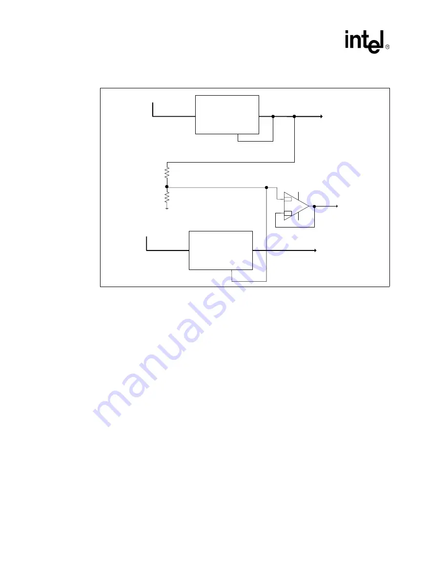
+V_1.25 may optionally be on the switch rail and turned off in either S3 or S4. This is only a block
diagram. It is the responsibility of the system designer to ensure that the timing requirements for
the DDR memory devices and GMCH are met.
4.8.2.1
2.5 V Power Delivery Guidelines
The 2.5 V power for the GMCH system memory interface and the DDR DIMMs is delivered
around the DDR command, control, and clock signals. Special attention must be paid to the 2.5 V
copper flooding to ensure proper GMCH and DIMM power delivery. This 2.5 V flood must extend
from the GMCH 2.5 V power vias all the way to the 2.5 V DDR voltage regulator and its bulk
capacitors. The 2.5 V DDR voltage regulator must connect to the 2.5 V flood with a minimum of
six vias. The DIMM connector 2.5 V pins as well as the GMCH 2.5 V power vias must connect to
the 2.5 V copper flood.
In the areas where the copper flooding necks down around the GMCH make sure to keep these
neck down lengths as short as possible. The 2.5 V copper flooding under the DIMM connectors
must encompass all the DIMM 2.5 V pins and must be solid except for the small areas where the
clocks are routed within the DIMM pin field to their specified DIMM pins.
Note:
A minimum of 12 mil isolation spacing shall be maintained between the copper flooding and any
signals on the same layer.
depicts the voltage and current specifications for each the GMCH and memory reference
and termination voltages. For convenience, tolerances are given in both percentage and volts,
although validation shall be done using the specifications exactly as they are written. When the
Figure 52. DDR Power Delivery Block Diagram
Vin
Vout
Sense Adj.
Switching
Regulator
Vin
Vout
Sense Adj.
Switching
Regulator
50 - 150
Ω
+V5
+V2_5
+V5
+V1_25
+
-
SMVREF
50 - 150
Ω
Содержание 6300ESB ICH
Страница 24: ...24 Intel 855GME Chipset and Intel 6300ESB ICH Embedded Platform Design Guide Introduction...
Страница 36: ...36 Intel 855GME Chipset and Intel 6300ESB ICH Embedded Platform Design Guide General Design Considerations...
Страница 102: ...102 Intel 855GME Chipset and Intel 6300ESB ICH Embedded Platform Design Guide...
Страница 122: ...122 Intel 855GME Chipset and Intel 6300ESB ICH Embedded Platform Design Guide...
Страница 152: ...152 Intel 855GME Chipset and Intel 6300ESB ICH Embedded Platform Design Guide System Memory Design Guidelines DDR SDRAM...
Страница 172: ...172 Intel 855GME Chipset and Intel 6300ESB ICH Embedded Platform Design Guide Integrated Graphics Display Port...
Страница 190: ...190 Intel 855GME Chipset and Intel 6300ESB ICH Embedded Platform Design Guide Hub Interface...
Страница 246: ...246 Intel 855GME Chipset and Intel 6300ESB ICH Embedded Platform Design Guide Intel 6300ESB Design Guidelines...
Страница 264: ...264 Intel 855GME Chipset and Intel 6300ESB ICH Embedded Platform Design Guide Platform Clock Routing Guidelines...
Страница 298: ...298 Intel 855GME Chipset and Intel 6300ESB ICH Embedded Platform Design Guide Schematic Checklist Summary...
Страница 318: ...318 Intel 855GME Chipset and Intel 6300ESB ICH Embedded Platform Design Guide Layout Checklist...


