Document Number: 002-14826 Rev. *G
Page 53 of 65
PRELIMINARY
CYW43903
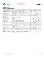
15.5 BBPLL LDO
Table 29. BBPLL LDO Specifications
Parameter
Conditions and Comments
Min.
Typ.
Max.
Units
Input supply voltage, V
in
Min. V
in
= V
o
+ 0.15V = 1.35V (for V
o
= 1.2V).
The dropout voltage requirement must be met under maximum
load.
1.3
1.35
1.5
V
Output voltage, V
o
Programmable in 25 mV steps. Default = 1.2V.
1.1
1.2
1.275
V
Dropout voltage
At max. load
–
–
150
mV
Output voltage DC
accuracy
Includes line/load regulation.
–4
–
+4
%
Output current
Peak load = 80 mA, average = 35 mA
0.1
–
55
mA
Quiescent current
No load
–
10
12
μA
55 mA load
–
550
570
μA
Line regulation
V
in
from (V
o
+ 0.15V) to 1.5V; 200 mA load
–
–
5
mV/V
Load regulation
load from 1mA to 200 mA; V
in
≥ (V
o
+ 0.15V)
–
0.025
0.045
mV/mA
Leakage current
Powered down. Junction temperature is 85°C.
–
5
20
μA
Bypass mode
–
0.2
1.5
μA
PSRR
@1 kHz, V
in
≥ V
o
+ 0.15V, Co = 4.7 μF
20
–
–
dB
Start-up time of PMU
VIO up and steady. Time from REG_ON rising edge to CLDO
reaching 99% of V
o
.
–
530
700
us
LDO turn-on time
The LDO turn-on time when the rest of the chip is up.
–
140
180
us
Inrush current
Vin=Vo+0.15V to 1.5V, Co=0.47uF, no load
–
60
70
mA
External output capacitor,
C
o
Ceramic, X5R, size 0201, max. 6.3V, 20% tolerance
0.27
0.47
–
μF
External input capacitor
Only use an external input capacitor at the LDO_VDD1P5 pin if it
is not supplied from the CBUCK output.
–
1
–
μF


