Document Number: 002-14826 Rev. *G
Page 16 of 65
PRELIMINARY
CYW43903
4. Applications Subsystem
4.1 Overview
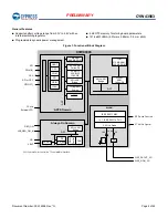
The Applications subsystem contains the general use CPU, memory, the standalone DMA core, the cryptography core, and the
majority of the external interfaces.
4.2 Applications CPU and Memory Subsystem
This subsystem has an integrated 32-bit ARM Cortex-R4 processor with an internal 32 KB D-cache and an internal 32 KB I-cache.
The ARM Cortex-R4 is a low-power processor that features a low gate count, low interrupt latency, and low-cost debugging capabil-
ities. It is intended for deeply embedded applications that require fast interrupt response features. The ARM Cortex-R4 implements
the ARM v7-R architecture and supports the Thumb-2 instruction set.
At 0.19 µW/MHz, the Cortex-R4 is the most power efficient general-purpose microprocessor available, outperforming 8- and 16-bit
devices on a MIPS/µW basis. It also supports integrated sleep modes.
Using multiple technologies to reduce cost, the ARM Cortex-R4 enables improved memory utilization, reduced pin overhead, and
reduced silicon area. It also has extensive debugging features, including real-time tracing of program execution.
On-chip memory for the CPU includes 1 MB SRAM, 640 KB ROM, and an 8 KB RAM powered independently of the application
subsystem.
4.3 Memory-to-Memory DMA Core
The CYW43903 memory-to-memory DMA (M2MDMA) engine contains eight DMA channel pairs, each containing one transmit/pull
engine and one receive/push engine.
The DMA engine provides general purpose data movement between memories that can be on the device, attached directly to the
device, or accessed through a host interface. The transmit/pull engine reads data from the source memory and immediately passes
it to the paired receive/push engine, which proceeds to write it to the destination memory. Multiple masters can program the individual
channels, and multiple interrupts are provided so that interrupts for different channels can be routed separately to different masters.
4.4 Cryptography Core
This core provides general purpose data movement between memories, which may be either on the device, attached directly to the
device, or accessed through a host interface. The transmit/pull engine reads data from the source memory and passes it immediately
to the paired receive/push engine that proceeds to write it to the destination memory. Multiple masters may program the individual
channels, and multiple interrupts are provided so that interrupts for different channels can be routed separately to different masters.
The cryptography block provides a hardware accelerator for enciphering and deciphering data that has undergone processing using
standards-based encryption algorithms. The cryptography block includes the following primary features:
■
Encryption and hash engines that support single pass AUTH-ENC or ENC-AUTH processing.
■
A scalable AES module that supports CBC, ECB, CTR, CFB, OFB, and XTS encryption with 128-, 192-, and 256-bit key sizes.
■
A scalable DES module that supports DES and 3DES in ECB and CBC modes.
■
An RC4 stream cipher module that supports state initialization, state update, and key-stream generation.
■
MD5, SHA1, SHA224, and SHA256 engines that support pure hash or HMAC operations.
■
A built-in 512-byte key cache for locally protected key storage.
OTP memory is used to store authentication keys.

