Application Note
19 of 27
V 1.0
2021-04-30
CoolGaN™ IPS half-bridge evaluation board with IGI60F1414A1L
Setup and use
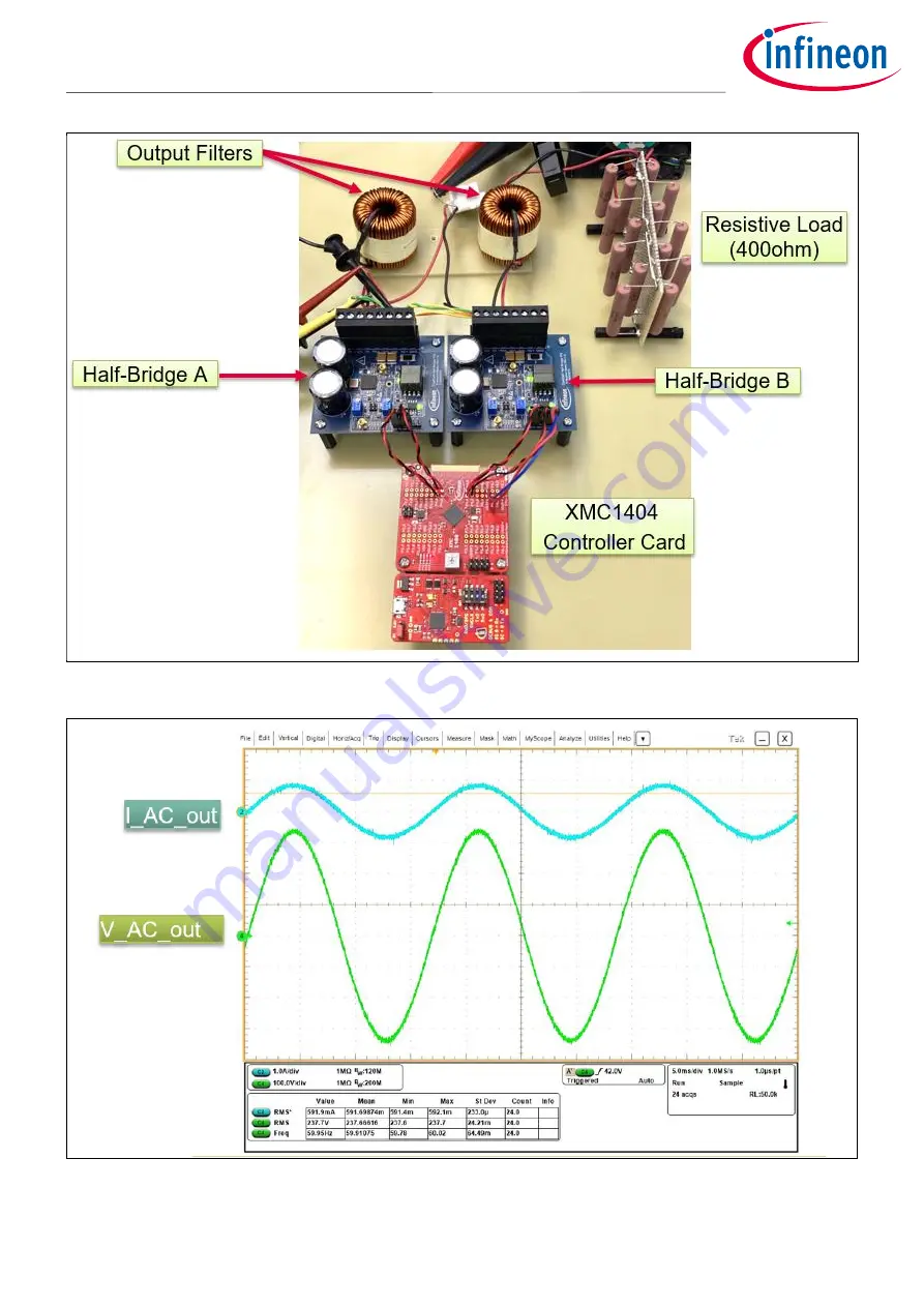
Figure 23
Inverter setup with two half-bridge evaluation boards
Figure 24
Inverter voltage and current output
Страница 1: ...c that provides adjustable dead time Additionally the board provides direct access to the logic inputs of the CoolGaN IPS chipset to drive the chipset with an external microcontroller or digital signa...
Страница 2: ...de gate driver 7 3 4 Half bridge output circuit 8 4 Setup and use 9 4 1 Test equipment needed 9 4 2 Connections to the terminal block 9 4 2 1 Connections for double pulse testing 10 4 2 2 Connections...
Страница 3: ...The output and bus voltage can range up to 450 V which is limited by the capacitor rating This half bridge can switch continuous currents of 4 A and peak currents of 10 A hard or soft switching Depen...
Страница 4: ...utput An oscilloscope is used to observe and measure the inductor current with a current probe switch node voltage or any other signal on the hardware board Table 2 includes all the available test poi...
Страница 5: ...node is connected to Vin Make sure that the jumpers on P1 header is placed to apply the PWMs to the IPS chipset shown in Figure 5 The outputs can be observed from TP1 and TP2 Figure 4 Input logic and...
Страница 6: ...t is user s responsibility to make sure that simultaneous turn on for both high and low signal will not happen In case of using microcontroller PWM a minimum deadtime of 50 nS is recommended Figure 5...
Страница 7: ...gate driver is supplied by the isolated gate driver power supply VDD_LS with about 8 V The RRC network for this channel consist of R17 R19 and C17 Additionally a fast turn off circuit including D9 an...
Страница 8: ...o discharge the DC bus capacitors after disconnecting from the source Attention Do not rely on the lab power supply discarding capability when shutting it off Always ensure that the capacitors are dis...
Страница 9: ...nd keep them below 450 V Use lab test power supply with current limit and set it in a proper value to avoid catastrophic damage to the board in case of any failure Eye and ear protection is recommende...
Страница 10: ...he PWM applied to the J1 If a resistive load is applied and the inductor current is above the boundary condition continuous current mode then the high side will turn on in a hard switching condition T...
Страница 11: ...t descriptions Test point label Description TP1 Input to the high side logic of the IPS INH TP2 Input to the low side logic of the IPS INL TP3 PWM input parallel to J1 Typical levels here should be 0...
Страница 12: ...pply 4 6 Verifying and adjusting deadtime For adjusting and trimming the deadtime refer to section 4 6 in reference 1 Figure 12 and Figure 13 show the adjusted 100 ns deadtime in rising and falling ed...
Страница 13: ...the next step adding the external inductor for desired test topology This example shows how to setup the board for buck topology testing Before powering up you may want to observe the gate voltages Fi...
Страница 14: ...he inductor current Note that both the gate and drain voltages are clean with minimal ringing or overshoot even though the switching speed is fast Temperature of the chipset and heatsink can be monito...
Страница 15: ...ng 125 C on chipset case temperature To increase the power dissipation capability of the chipset a heatsink can be attached to the bottom side of the PCB in the marked area beneath the chipset shown i...
Страница 16: ...C bus the output settles at 200 V and the peak peak current will be about 5 AMP The expanded view is shown in Figure 20 Both high and low side GaN transistors are operating in ZVS mode with about 8 V...
Страница 17: ...drive the half bridges with Sine PWM unipolar pattern The generated output line frequency is 60 Hz and the switching frequency is 65 kHz For this test there is no closed loop control only open loop in...
Страница 18: ...Application Note 18 of 27 V 1 0 2021 04 30 CoolGaN IPS half bridge evaluation board with IGI60F1414A1L Setup and use Figure 22 Inverter setup with two half bridge evaluation boards...
Страница 19: ...ote 19 of 27 V 1 0 2021 04 30 CoolGaN IPS half bridge evaluation board with IGI60F1414A1L Setup and use Figure 23 Inverter setup with two half bridge evaluation boards Figure 24 Inverter voltage and c...
Страница 20: ...Application Note 20 of 27 V 1 0 2021 04 30 CoolGaN IPS half bridge evaluation board with IGI60F1414A1L Setup and use Figure 25 Thermal image of the half bridge A...
Страница 21: ...lication Note 21 of 27 V 1 0 2021 04 30 CoolGaN IPS half bridge evaluation board with IGI60F1414A1L Complete schematic 5 Complete schematic Figure 26 Schematic of CoolGaN IPS half bridge evaluation bo...
Страница 22: ...IPS half bridge evaluation board with IGI60F1414A1L PCB layout 6 PCB layout The evaluation board is 1 3 mm thick with 4 layers 70 m thick copper The layer stackup is depicted below Figure 27 Top laye...
Страница 23: ...Application Note 23 of 27 V 1 0 2021 04 30 CoolGaN IPS half bridge evaluation board with IGI60F1414A1L PCB layout Figure 29 Lower middle copper layer Figure 30 Bottom copper layer...
Страница 24: ...y Diode Not Populated 3 ES1JLR3GCT ND J1 J2 CONN MMCX JACK STR 50 OHM PCB 2 WM9481 ND LED1 LED2 LED3 LED GREEN CLEAR 0805 SMD 3 732 4986 1 ND P1 CONN HEADER VERT 4POS 2MM 1 0877580417 ND R1 R10 SMD 2...
Страница 25: ...n Note 25 of 27 V 1 0 2021 04 30 CoolGaN IPS half bridge evaluation board with IGI60F1414A1L References 8 References 1 Application note on CoolGaN 600 V half bridge evaluation platform featuring EiceD...
Страница 26: ...Note 26 of 27 V 1 0 2021 04 30 CoolGaN IPS half bridge evaluation board with IGI60F1414A1L Revision history Revision history Document version Date of release Description of changes V 1 0 30 04 2021 Fi...
Страница 27: ...intellectual property rights of any third party with respect to any and all information given in this application note The data contained in this document is exclusively intended for technically trai...