9. Resets, Clocks and Power-up Options
170
PowerSpan II User Manual
80A1010_MA001_09
Integrated Device Technology
www.idt.com
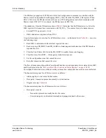
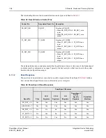
PowerSpan II assertion of P2_RST# occurs if P2_RST_DIR is pulled high and on of the following
occurs:
•
PO_RST_ asserted
•
PB_RST_DIR is pulled low and PB_RST_ is asserted
•
P1_RST_DIR is pulled low and P1_RST# is asserted
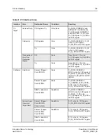
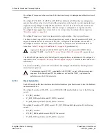
The negation of HEALTHY# tristates all PowerSpan II output pins, including the reset outputs.
PowerSpan II reset outputs do not respond immediately to the negation of PO_RST_ because they are
negated once all internal PLLs are locked.
9.2
Clocks
Each of the PowerSpan II external ports has a clock input pin. The pins are:
•
PB_CLK
•
P1_CLK
•
P2_CLK
The clock input for each port enables PowerSpan II’s master/target state machines to be synchronized
to the external bus. Each interface has a dedicated PLL designed to eliminate clock tree insertion delay.
PowerSpan II requires the input clock to be at the specified frequency before the negation of PO_RST_
(see
and
, parameter
t
102
). PowerSpan II PLLs are reset
during either the assertion of PO_RST_ or the negation of HEALTHY#. The PLLs are not locked until
a certain period after the negation of PO_RST_ or HEALTHY# (see
, parameter
t
103
).
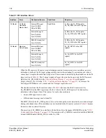
Each PLL has a dedicated configuration pin to indicate the desired operating frequency range. The
following configuration pins are used by the PLL:
•
PB_FAST
•
P1_M66EN
•
P2_M66EN
The input clocks are not required to maintain specific phase relationships. However, there is a
limitation on the range of input clock periods. The ratio of the maximum period to minimum period, for
all three clock inputs, must be less than four. For example, if the period of PB_CLK is 10 ns, the
periods of P1_CLK and P2_CLK must be less than, but not equal to, 40 ns.
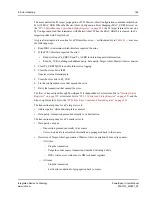
PowerSpan II has power-up options for bypassing all three PLLs. This capability is used for debugging
purposes. IDT recommends always enabling the PLL.Refer to
“Power-Up Options” on page 171
for
more information on power-up options.
PB_FAST, P1_M66EN, and P2_M66EN are multiplexed signals. They are also used for
PowerSpan II power-up options (see
“Power-Up Options” on page 171
).
Содержание PowerSpan II
Страница 8: ...Contents 8 PowerSpan II User Manual 80A1010_MA001_09 Integrated Device Technology www idt com ...
Страница 14: ...List of Tables 14 PowerSpan II User Manual 80A1010_MA001_09 Integrated Device Technology www idt com ...
Страница 18: ...About this Document 18 PowerSpan II User Manual 80A1010_MA001_09 Integrated Device Technology www idt com ...
Страница 82: ...2 PCI Interface 82 PowerSpan II User Manual 80A1010_MA001_09 Integrated Device Technology www idt com ...
Страница 112: ...3 Processor Bus Interface 112 PowerSpan II User Manual 80A1010_MA001_09 Integrated Device Technology www idt com ...
Страница 156: ...7 Interrupt Handling 156 PowerSpan II User Manual 80A1010_MA001_09 Integrated Device Technology www idt com ...
Страница 380: ...12 Register Descriptions 380 PowerSpan II User Manual 80A1010_MA001_09 Integrated Device Technology www idt com ...
Страница 394: ...14 Package Information 394 PowerSpan II User Manual 80A1010_MA001_09 Integrated Device Technology www idt com ...
Страница 414: ...15 AC Timing 414 PowerSpan II User Manual 80A1010_MA001_09 Integrated Device Technology www idt com ...
Страница 416: ...16 Ordering Information 416 PowerSpan II User Manual 80A1010_MA001_09 Integrated Device Technology www idt com ...
Страница 420: ...A Hardware Implementation 420 PowerSpan II User Manual 80A1010_MA001_09 Integrated Device Technology www idt com ...
Страница 428: ...B Typical Applications 428 PowerSpan II User Manual 80A1010_MA001_09 Integrated Device Technology www idt com ...
Страница 432: ...Glossary 432 PowerSpan II User Manual 80A1010_MA001_09 Integrated Device Technology www idt com ...


