3. Processor Bus Interface
103
PowerSpan II User Manual
80A1010_MA001_09
Integrated Device Technology
www.idt.com
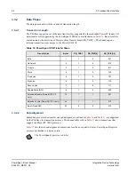
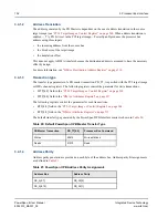
During PB master transactions, PB_AP[0:3] is driven to the correct values for either even parity or odd
parity. Odd versus even parity is controlled with the PARITY bit in the
Control and Status Register” on page 304
.
3.4.2
Data Phase
The data phase deals with arbitration for the data bus, and control of transaction size and length.
3.4.2.1
Data Bus Arbitration and Tenure
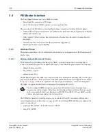
The PB Master generates a data bus request by driving Transfer Type (PB_TT[3]) high during assertion
of Transfer Start (PB_TS_). The PB Master asserts Data Bus Busy (PB_DBB_) to indicate data bus
ownership when it receives a qualified bus grant (see
). A qualified bus grant
includes:
•
Data Bus Grant (DBG) signal asserted
•
PB_ARTRY_ negated
•
Data bus not busy
The PB Master negates PB_DBB_ for at least one clock after the final data termination signal is
asserted by the slave.
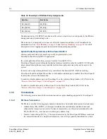
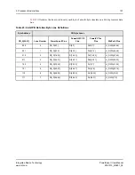
PB_A[16:23]
PB_AP[2]
PB_A[24:31]
PB_AP[3]
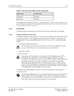
If the DBG signal is asserted past the data tenure of a transaction, the PB Master sees the
assertion of the DBG signal as a new data tenure and re-asserts PB_DBB_.
External slaves must not indicate a successful data transfer with the assertion of PB_TA_
and/or PB_DVAL_ earlier than two clocks after the assertion of PB_TS_. To ensure
PowerQUICC II compliance with this rule, the PowerQUICC II register BCR[APD] must be
programed to a value greater than one. This parameter specifies the earliest time after
assertion of PB_TS_ that the PowerQUICC II slave asserts PB_TA_ to complete a data
transfer. The BCR[APD] parameter is supported by the PowerQUICC II to accommodate
processor bus agents with a range of snoop response times. BCR[APD] must be programmed
to accommodate the slowest snooping device in the system.
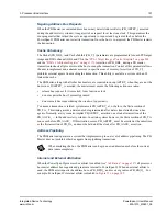
The PowerSpan II PB Master derives equivalent Data Bus Busy information from PB control
signals. This allows the PowerSpan II processor bus arbiter to operate in processor bus
environments that do not implement DBB. Some processors (for example the PowerQUICC
II) use DBB to qualify data bus grants generated by the system arbiter.
Table 21: PowerSpan II PB Address Parity Assignments
Address Bus
Address Parity
Содержание PowerSpan II
Страница 8: ...Contents 8 PowerSpan II User Manual 80A1010_MA001_09 Integrated Device Technology www idt com ...
Страница 14: ...List of Tables 14 PowerSpan II User Manual 80A1010_MA001_09 Integrated Device Technology www idt com ...
Страница 18: ...About this Document 18 PowerSpan II User Manual 80A1010_MA001_09 Integrated Device Technology www idt com ...
Страница 82: ...2 PCI Interface 82 PowerSpan II User Manual 80A1010_MA001_09 Integrated Device Technology www idt com ...
Страница 112: ...3 Processor Bus Interface 112 PowerSpan II User Manual 80A1010_MA001_09 Integrated Device Technology www idt com ...
Страница 156: ...7 Interrupt Handling 156 PowerSpan II User Manual 80A1010_MA001_09 Integrated Device Technology www idt com ...
Страница 380: ...12 Register Descriptions 380 PowerSpan II User Manual 80A1010_MA001_09 Integrated Device Technology www idt com ...
Страница 394: ...14 Package Information 394 PowerSpan II User Manual 80A1010_MA001_09 Integrated Device Technology www idt com ...
Страница 414: ...15 AC Timing 414 PowerSpan II User Manual 80A1010_MA001_09 Integrated Device Technology www idt com ...
Страница 416: ...16 Ordering Information 416 PowerSpan II User Manual 80A1010_MA001_09 Integrated Device Technology www idt com ...
Страница 420: ...A Hardware Implementation 420 PowerSpan II User Manual 80A1010_MA001_09 Integrated Device Technology www idt com ...
Страница 428: ...B Typical Applications 428 PowerSpan II User Manual 80A1010_MA001_09 Integrated Device Technology www idt com ...
Страница 432: ...Glossary 432 PowerSpan II User Manual 80A1010_MA001_09 Integrated Device Technology www idt com ...


