


Rev. 1.00
�07 of ���
�an�a�� 1�� �01�
Standard 8051 8-Bit Flash MCU
HT85F2260/HT85F2270/HT85F2280
UART Serial Interfaces – UART0 and UART1
UART Serial Interfaces – UART0 and UART1
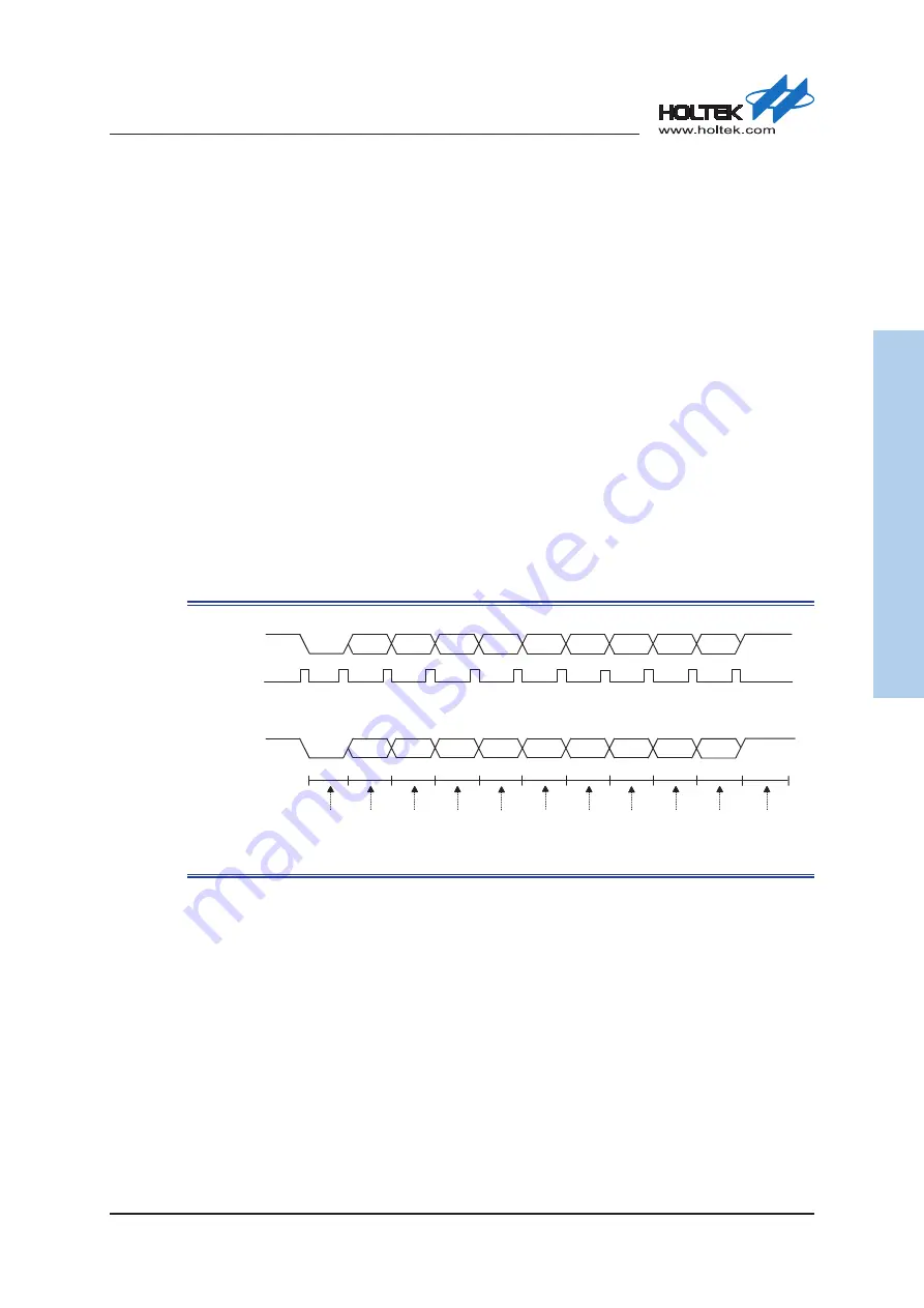
Mode 3
The only difference between Mode 2 and Mode 3 is that the internal Baud rate is variable in
Mode 3, whereas it is fixed in Mode 2. Mode 3 is an integrated full-duplex asynchronous serial
communication interface. The 9 bits of data are received via the RXD0 pin while the TXD0 pin
is the data transmit pin for this communication mode. For data reception, data received on the
RXD0 pin will be shifted into the Receive Shift Register by the Baud rate generator. For data
transmission, data in the Transmit Shift Register will be will be shifted out onto the TXD0 pin by
the Baud rate generator. The Baud rate frequency is selected by the BD bit in the SBRCON register
to be either sourced from the Timer1 overflow or to be setup by the S0RELL/S0RELH registers. In
addition, the Baud rate can be doubled using the SMOD bit in the PCON register.
Data transmission is started by writing to the S0BUF register. The TXD0 pin outputs the serial
data. The first bit transmitted is a start bit, always “0”, then 9 bits of data where the 9th bit is taken
from the TB80 bit of the S0CON register, after which a stop bit, always “1”, is transmitted.
Data to be received by the UART is accepted on the external RXD0 pin. When reception starts, the
UART0 synchronizes with the falling edge detected by the RXD0 pin. Input data is available after
one byte of data is complete in the S0BUF register, and the 9th bit is available as the RB80 bit in
the S0CON register. During the reception process, the S0BUF data and the RB80 bit will remain
unchanged until the process is complete.
UART0 Mode 3 Timing Diagram