


Rev. 1.00
1�8 of ���
�an�a�� 1�� �01�
Standard 8051 8-Bit Flash MCU
HT85F2260/HT85F2270/HT85F2280
Analog to Digital Converter –
ADC
A/D Converter Clock Source
The clock source for the A/D converter, which originates from the system clock f
SYS
, can be chosen
to be either f
SYS
or a subdivided version of f
SYS
. The division ratio value is determined by the
ADCK2~ADCK0 bits in the ADCR1 register.
Although the A/D clock source is determined by the system clock f
SYS
, and by bits ADCK2~ADCK0,
there are some limitations on the maximum A/D clock source speed that can be selected. As the
minimum value of permissible A/D clock period, t
ADCK
, is 0.5μs, care must be taken for system
clock frequencies equal to or greater than 4MHz. For example, if the system clock operates at a
frequency of 4MHz, the ADCK2~ADCK0 bits should not be set to “000”. Doing so will give A/D
clock periods that are less than the minimum A/D clock period which may result in inaccurate A/D
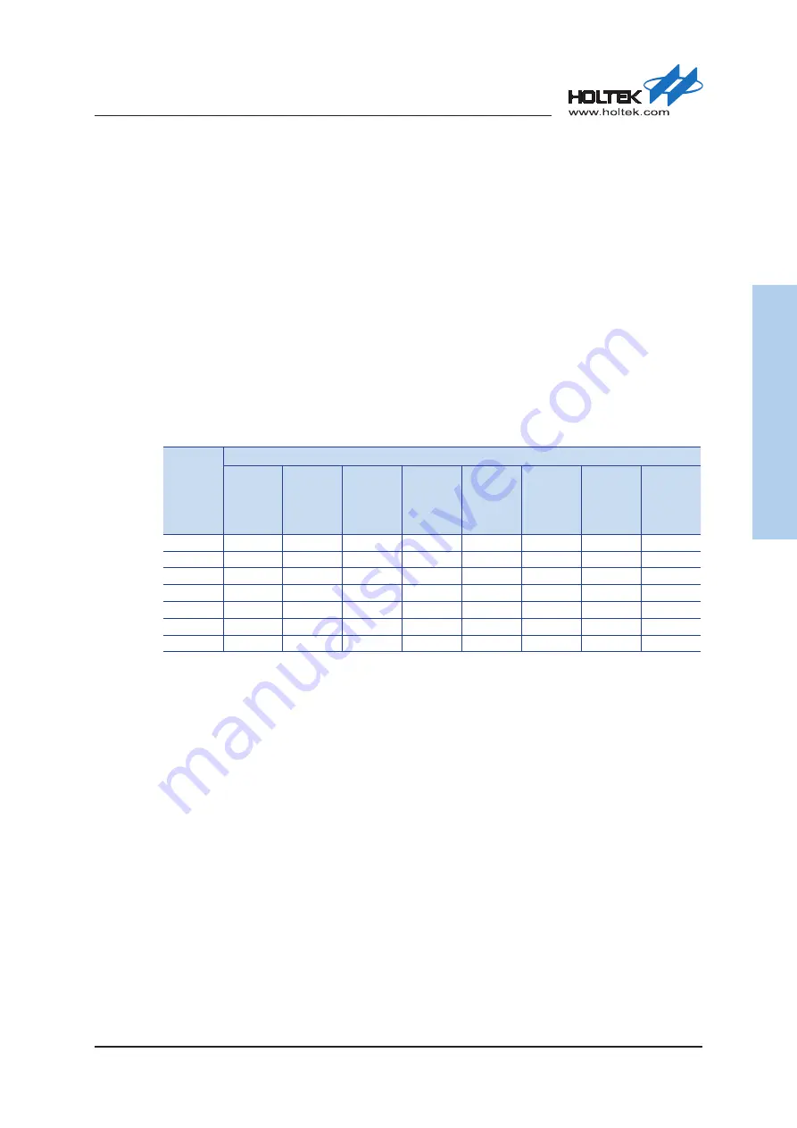
conversion values. Refer to the following table for examples, where values marked with an asterisk
* show where, depending upon the device, special care must be taken, as the values may be less
than the specified minimum A/D Clock Period.
A/D Clock Period Examples
f
SYS
A/D Clock Period (t
ADCK
)
ADCK2,
ADCK1,
ADCK0
=000
(f
SYS
)
ADCK2,
ADCK1,
ADCK0
=001
(f
SYS
/2)
ADCK2,
ADCK1,
ADCK0
=010
(f
SYS
/4)
ADCK2,
ADCK1,
ADCK0
=011
(f
SYS
/8)
ADCK2,
ADCK1,
ADCK0
=100
(f
SYS
/16)
ADCK2,
ADCK1,
ADCK0
=101
(f
SYS
/32)
ADCK2,
ADCK1,
ADCK0
=110
(f
SYS
/64)
ADCK2,
ADCK1,
ADCK0
=111
1MHz
1μs
2μs
4μs
8μs
16μs
32μs
64μs
Undefined
�MHz
�00ns
1μs
2μs
4μs
8μs
16μs
32μs
Undefined
4MHz
��0ns*
�00ns
1μs
2μs
4μs
8μs
16μs
Undefined
8MHz
1��ns*
��0ns*
�00ns
1μs
2μs
4μs
8μs
Undefined
1�MHz
83ns*
167ns*
333ns*
667ns
1.33μs
2.67μs
5.33μs
Undefined
16MHz
6�.�ns*
1��ns*
��0ns*
�00ns
1μs
2μs
4μs
Undefined
3�MHz
31.��ns*
6�.�ns*
1��ns*
��0ns*
�00ns
1μs
2μs
Undefined
A/D Input Pins
All of the A/D analog input pins are pin-shared with the I/O pins on Port 4 function. The
ACE7~ACE0 bits in the ADCR2 registers, determine whether the input pins are setup as A/D
converter analog inputs or I/O function. If the ACE7~ACE0 bits for its corresponding pin is set
high then the pin will be setup to be an A/D converter input and the original pin functions disabled.
In this way, pins can be changed under program control to change their function between A/D
inputs and I/O function. All pull-high resistors, which are setup through register programming,
will be automatically disconnected if the pins are setup as A/D inputs. Note that it is not necessary
to first setup the A/D pin as an input in the P4 port control register to enable the A/D input as when
the ACE7~ACE0 bits enable an A/D input, the status of the port control register will be overridden.
The A/D converter has its own reference voltage pin, VREF, however the reference voltage can
also be supplied from the power supply pin or internal voltage reference, a choice which is made
through the VREFAS and VREFIS bits in the ADCR1 register. The analog input values must not
be allowed to exceed the value of V
REF
.