


Rev. 2.10
�2
���� 02� 201�
Rev. 2.10
�3
���� 02� 201�
HT68F20/HT68F30/HT68F40/HT68F50/HT68F60
HT68FU30/HT68FU40/HT68FU50/HT68FU60
Enhanced I/O Flash Type 8-Bit MCU with EEPROM
HT68F20/HT68F30/HT68F40/HT68F50/HT68F60
HT68FU30/HT68FU40/HT68FU50/HT68FU60
Enhanced I/O Flash Type 8-Bit MCU with EEPROM
EEPROM Data Memory
The device contains an area of internal EEPROM Data Memory. EEPROM, which stands for
Electrically Erasable Programmable Read Only Memory, is by its nature a non-volatile form
of re-programmable memory, with data retention even when its power supply is removed. By
incorporating this kind of data memory, a whole new host of application possibilities are made
available to the designer. The availability of EEPROM storage allows information such as product
identification numbers, calibration values, specific user data, system setup data or other product
information to be stored directly within the product microcontroller. The process of reading and
writing data to the EEPROM memory has been reduced to a very trivial affair.
EEPROM Data Memory Structure
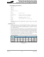
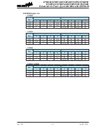
The EEPROM Data Memory capacity varies from 32×8 to 256×8 bits, according to the device
selected. Unlike the Program Memory and RAM Data Memory, the EEPROM Data Memory is not
directly mapped into memory space and is therefore not directly addressable in the same way as the
other types of memory. Read and Write operations to the EEPROM are carried out in single byte
operations using an address and data register in Bank 0 and a single control register in Bank 1.
Device
Capacity
Address
HT68F20
32×8
00H~1FH
HT68F30
6�×8
00H~3FH
HT68F�0
128×8
00H~7FH
HT68F50/HT68F60
256×8
00H~FFH
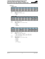
EEPROM Registers
Three registers control the overall operation of the internal EEPROM Data Memory. These are the
address register, EEA, the data register, EED and a single control register, EEC. As both the EEA
and EED registers are located in Bank 0, they can be directly accessed in the same was as any other
Special Function Register. The EEC register however, being located in Bank1, cannot be directly
addressed directly and can only be read from or written to indirectly using the MP1 Memory Pointer
and Indirect Addressing Register, IAR1. Because the EEC control register is located at address 40H
in Bank 1, the MP1 Memory Pointer must first be set to the value 40H and the Bank Pointer register,
BP, set to the value, 01H, before any operations on the EEC register are executed.


