


3 Development Board Circuit
3.12 AD/DA
DBUG375-1.2E
22(34)
3.12
AD/DA
3.12.1
Introduction
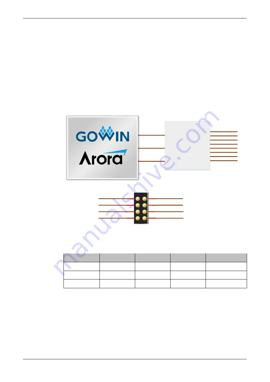
The AD/DA module uses a chip that is a 12-bit A/D and D/A converter
with configurable 8-channel interface, which can be configured as any
combination of ADC/DAC/GPIO and shares the I2C bus with the RTC
module. The input and output interface uses 8pin, and the connection
diagram is follows.
Figure 3-12 Connection Diagram of AD/DA
IIC_SDA
RTC_CLK
AD/DA_A0
AD/DA_D0
AD/DA_D1
AD/DA_D2
AD/DA_D3
AD/DA_D4
AD/DA_D5
AD/DA_D6
AD/DA_D7
AD/DA
Module
1
3
5
7
2
4
6
8
AD/DA_D0
AD/DA_D1
AD/DA_D2
AD/DA_D3
AD/DA_D4
AD/DA_D5
AD/DA_D6
AD/DA_D7
3.12.2
Pinout
Table 3-14 AD/DA Pinout
Name
FPGA Pin No. BANK
I/O Level
Description
AD/DA_A0
E14
1
2.5V
Address input
IIC_SCL
A13
1
2.5V
I2C signal
IIC_SDA
C13
1
2.5V
I2C signal
3.13
CAN
3.13.1
Introduction
The FPGA communicates with the transceiver via the UART interface,
and the maximum transmission rate is 1Mbps. The connection diagram is
as follows.
Содержание DK-START-GW2A55-PG484 V1.3
Страница 1: ...DK START GW2A55 PG484_V1 3 User Guide DBUG375 1 2E 09 01 2021 ...
Страница 44: ......


