


GD32E23x User Manual
301
Step2:
Compare mode configuration.
Set the shadow enable mode by CHxCOMSEN.
Set the output mode (set/clear/toggle) by CHxCOMCTL.
Select the active polarity by CHxP.
Enable the output by CHxEN.
Step3:
Interrupt/DMA-request enables configuration by CHxIE/CxCDE.
Step4:
Compare output timing configuration by TIMERx_CAR and TIMERx_CHxCV.
The TIMERx_CHxCV can be changed onging to meet the expected waveform.
Step5:
Start the counter by configuring CEN to 1.
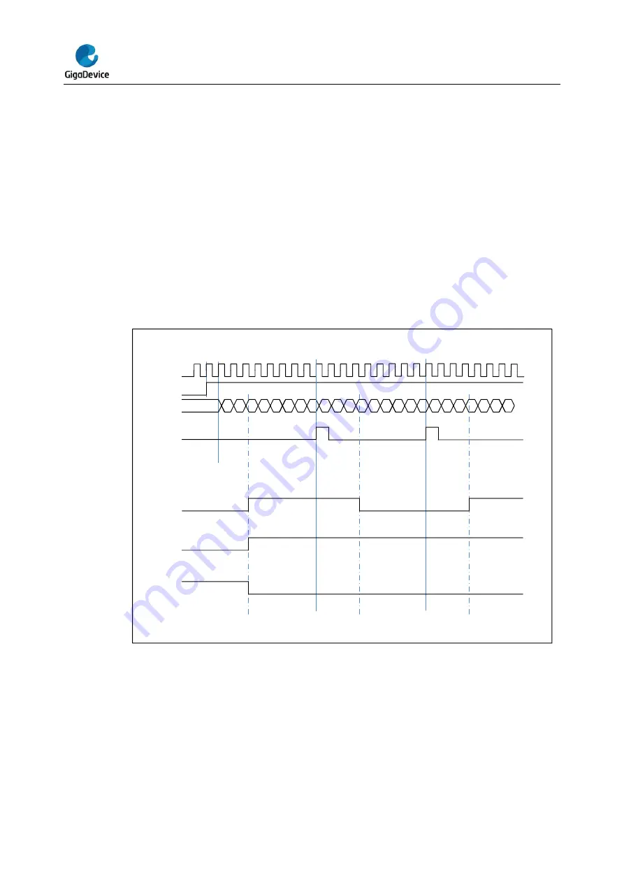
The timing chart below shows the three compare modes toggle/set/clear. CAR=0x63,
CHxVAL=0x3
Figure 14-41. Output-compare under three modes
CEN
CNT_REG
00
01
02
03
04
05
…
.
62
63
Overf low
match toggle
CNT_CLK
OxCPRE
00
01
02
03
04
05
…
.
62
63
01
02
03
04
05
…
.
00
match set
match clear
OxCPRE
OxCPRE
Output PWM function
In the output PWM function
(by setting the CHxCOMCTL bit to 3’b110 (PWM mode 0) or to
3’b 111(PWM mode 1)), the channel can generate PWM waveform according to the
TIMERx_CAR registers and TIMERx_CHxCV registers.
Based on the counter mode, PWM can also be divided into EAPWM (Edge-aligned PWM)
and CAPWM (Center-aligned PWM).
The
EAPWM’s period is determined by TIMERx_CAR and the duty cycle is determined


