


6
Rev NR
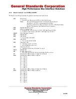
2.1.2
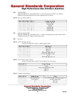
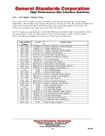
Board Control: Local Offset 0x0004
The Board Control Register defines the general control functions for the board.
D31
Board Reset
1 = Reset all Local Registers and FIFOs to their default values
Notes:
This bit will
automatically clear to 0 following the board reset.
Board Reset will NOT reset programmable oscillator.
Following a Board Reset, Reset-In-Progress bit (D31) of the Board Status
Register will remain set until the Board reset is complete;
D30
RESERVED (Debug Test)
D29
FIFO Test (Debug Test)
0 = Normal Mode - FIFO Write to Tx FIFO / FIFO Read from Rx FIFO
1 = Test Mode - FIFO Write to Rx FIFO / FIFO Read from Tx FIFO
D28:27
FIFO Allocation (Unused)
D26
RESERVED
D25
LED D1/D6
1 = Turn on Red LED D1/D6
D24
LED D1/D6
1 = Turn on Green LED D1/D6
D23
Timestamp Clear
0 = timestamp counter is enabled
1 = reset timestamp count to zero
D22
Timestamp Source
0 = timestamp counter runs off internal 1us clock
D21:9
RESERVED
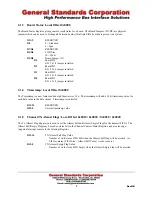
D8
Rx FIFO Stop on Full
1 = If Rx FIFO becomes full, stop receiving data (disable receiver).
D7
Demand Mode DMA Channel 1 Single Cycle Disable
D6:4
Demand Mode DMA Channel 1 Request
000 = Ch1 Rx
100 = Ch1 Tx
010 = Ch2 Rx
110 = Ch2 Tx
001 = Ch3 Rx
101 = Ch3 Tx
011 = Ch4 Rx
111 = Ch4 Tx
D3
Demand Mode DMA Channel 0 Single Cycle Disable
D2:0
Demand Mode DMA Channel 0 Request
000 = Ch1 Rx
100 = Ch1 Tx
010 = Ch2 Rx
110 = Ch2 Tx
001 = Ch3 Rx
101 = Ch3 Tx
011 = Ch4 Rx
111 = Ch4 Tx