Gamatronic Electronic Industries Ltd.
Power+ Technical Guide
7
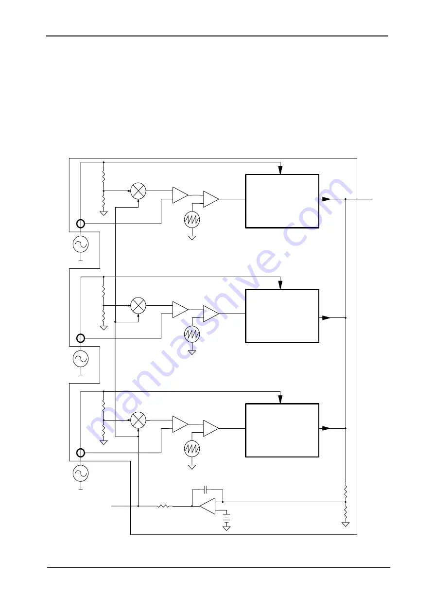
required for the proper operation, an inner current loop for maintaining a correct wave shape
and an outer voltage loop to ensure a correct DC output level.
The voltage sample (k*Vin) is multiplied by the error voltage from a common voltage feedback
amplifier (Integrator). The result is than compared to the actual sampled phase current which
forces the current amplifier current to follow the phase input voltage. The output of the
integrator is connected to a current sharing bus causing all other modules to be connected to
this bus via the same resistor. This ensures that all the multipliers of each UPS module receive
the same input and all that modules are equally loaded.
K2*Vout
Comparator
Triangle
NEUTRAL
MULT
Triangle
PWM
Comparator
Integarator
PH1
NEUTRAL
Current
Amplifier
Current
Amplifier
+
-
Vout (DC)
+
-
POWER
BLOCK
NEUTRAL
Comparator
POWER
BLOCK
Triangle
+
-
MULT
K1*V1
POWER
BLOCK
PWM
+
-
+
-
K1*V3
Current
Amplifier
+
-
K1*V2
PH3
Vref
PWM
MULT
Verror
PH2
DC
share
bus
+
-
Figure
2-5: PFC control scheme
Содержание POWER PLUS
Страница 13: ...Gamatronic Electronic Industries Ltd Power Technical Guide 5 Figure 2 2 Block diagram of a single UPS Module...
Страница 19: ...Gamatronic Electronic Industries Ltd Power Technical Guide 11 Figure 2 8 System controller Block diagram...
Страница 26: ...Gamatronic Electronic Industries Ltd 18 Power Technical Guide Figure 3 4 POWER System Rear View...


